Pixel array and manufacturing method thereof, and organic light emitting diode array substrate

A pixel array and pixel technology, applied in vacuum evaporation plating, instruments, static indicators, etc., can solve the problems that the pixel density cannot be greatly improved, the Mask opening cannot be made very small, and the arrangement density cannot be increased.

Active Publication Date: 2016-07-20
BOE TECH GRP CO LTD
View PDF6 Cites 28 Cited by
  • Summary
  • Abstract
  • Description
  • Claims
  • Application Information

AI Technical Summary

Problems solved by technology

[0004] Due to the lower limit of the opening area of ​​the mask, and in order to avoid the influence of tolerance in the manufacturing process, it is necessary to reserve enough gaps between the openings of adjacent pixels, so that the pixel density cannot be greatly increased.
Moreover, sub-pixels of different ...

Method used


Image

  • Pixel array and manufacturing method thereof, and organic light emitting diode array substrate
  • Pixel array and manufacturing method thereof, and organic light emitting diode array substrate
  • Pixel array and manufacturing method thereof, and organic light emitting diode array substrate

Examples


Embodiment Construction

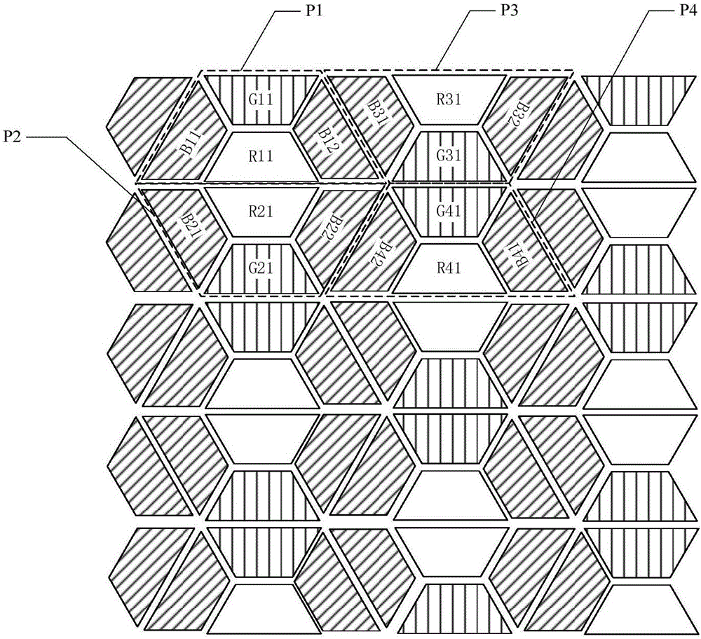
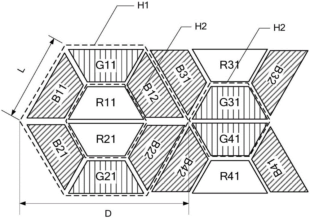
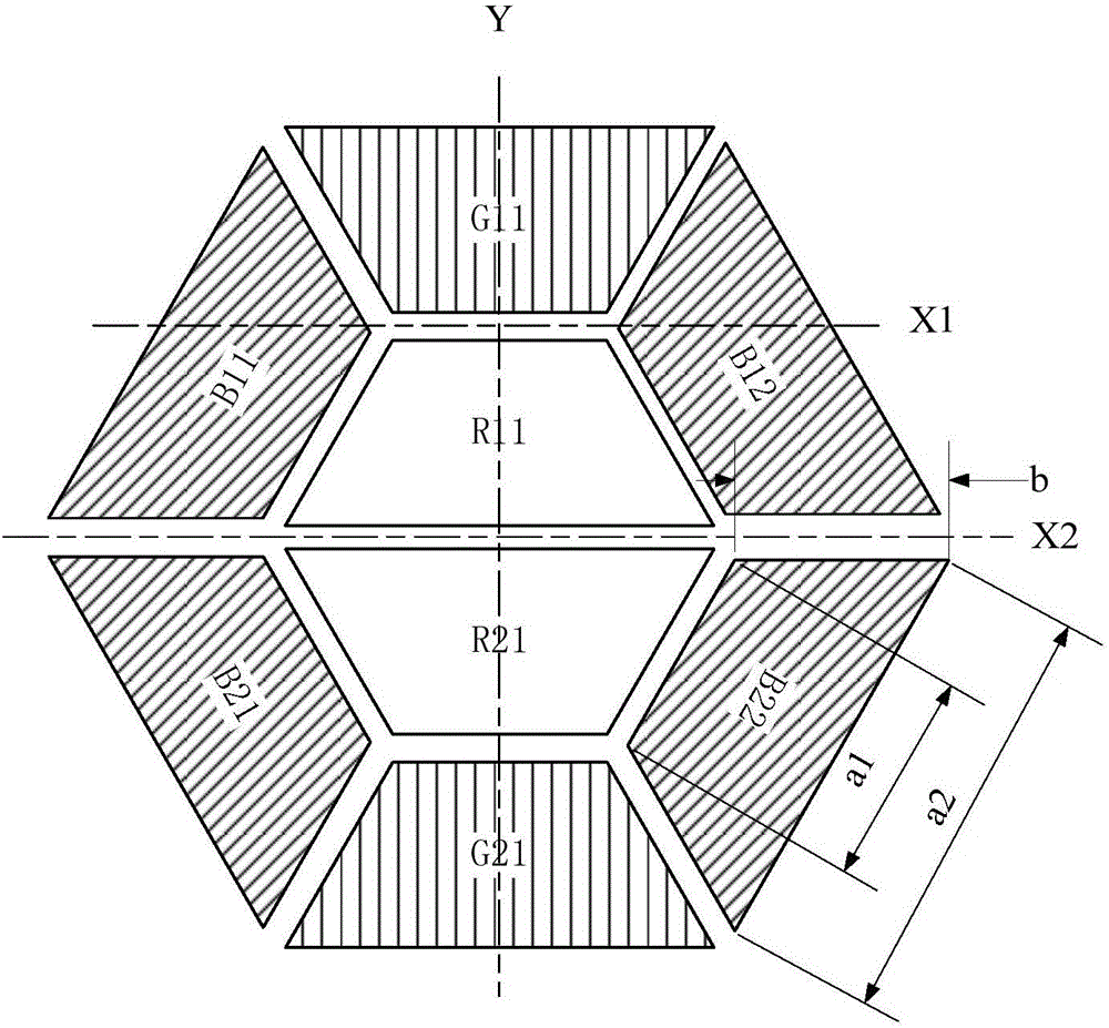
[0018] In order to make the purpose, technical solutions and advantages of the embodiments of the present disclosure clearer, the technical solutions of the embodiments of the present disclosure will be clearly and completely described below in conjunction with the accompanying drawings of the embodiments of the present disclosure. Apparently, the described embodiments are some of the embodiments of the present disclosure, not all of them. Based on the described embodiments of the present disclosure, all other embodiments obtained by persons of ordinary skill in the art without creative effort fall within the protection scope of the present disclosure.

[0019] Unless otherwise defined, the technical terms or scientific terms used herein shall have the usual meanings understood by those having ordinary skill in the art to which the present disclosure belongs. "First", "second" and similar words used in the specification and claims of the present disclosure do not indicate any ...


PUM


Abstract

A pixel array and a manufacturing method thereof, and an organic light emitting diode array substrate are disclosed. The pixel array comprises a plurality of pixels. Each pixel comprises four sub-pixels. Sizes of the four sub-pixels are the same and shapes of the four sub-pixels are an isosceles trapezoid. The four sub-pixels are arranged in a shape of a half of a regular hexagon. A display screen possessing the above structure has high rotation symmetry. A high resolution ratio and a high homogeneous degree can be acquired from each direction of the display screen.

Description

technical field [0001] The present disclosure relates to the field of display technology, in particular to a pixel array, a manufacturing method thereof, and an organic light emitting diode array substrate. Background technique [0002] The light-emitting structure of an organic light-emitting diode (Organic Light-Emitting Diode, OLED) device includes a pair of electrodes and an organic light-emitting layer. When a DC voltage is applied, holes are injected into the organic light-emitting layer from the anode, and electrons are injected into the organic light-emitting layer from the cathode. When it reaches the ground state, it will emit photons and emit light. [0003] There are many methods for manufacturing OLED displays, among which OLED evaporation technology is to form organic light-emitting devices by evaporating organic light-emitting materials and passing through high-precision metal masks (FineMetalMask, FMM) at positions corresponding to pixels on the array substr...

Claims


Application Information

Patent Timeline
IPC IPC(8): H01L27/32
CPCH10K59/353C23C14/042C23C14/12G09G2300/0452G09G3/3208H10K59/35H10K71/166H10K59/00H10K71/00
Inventor 杜小波
Owner BOE TECH GRP CO LTD
Why Eureka
Try Eureka