

Pixel structure
A pixel structure and pixel electrode technology, applied in nonlinear optics, instruments, optics, etc., can solve the problems of display panel contrast and decrease in transmittance, and achieve the effect of optimizing display characteristics
- Summary
- Abstract
- Description
- Claims
- Application Information
AI Technical Summary
Problems solved by technology
Method used
Image

Examples
no. 1 example
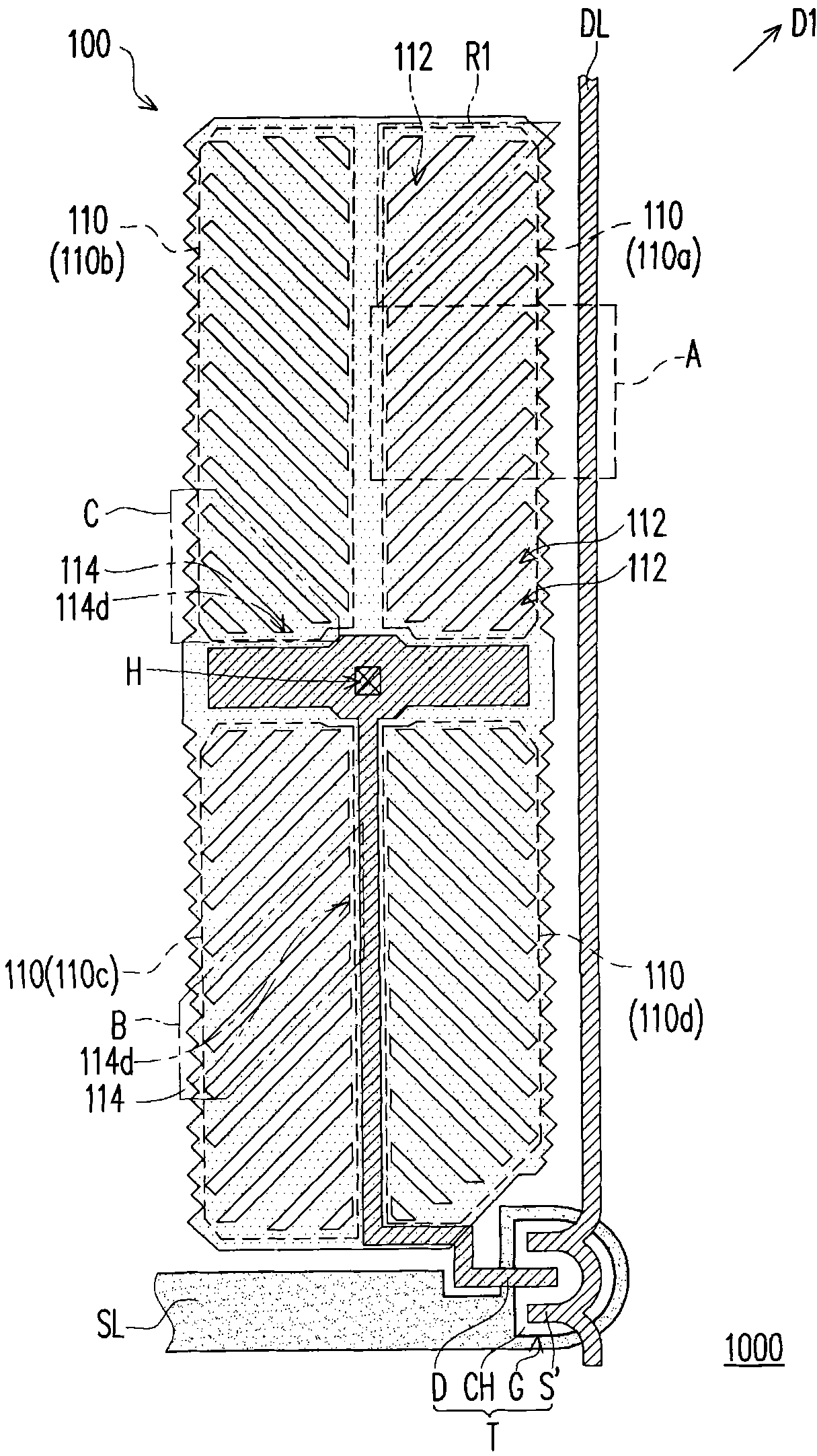
[0067] figure 2 It is a schematic top view of the pixel structure 1000 according to the first embodiment of the present invention. Please refer to figure 2, the pixel structure 1000 of this embodiment is suitable for being electrically connected to the scan line SL and the data DL. In this embodiment, the scan lines SL and the data lines DL are arranged alternately. In other words, the extending direction of the data lines DL is not parallel to the extending direction of the scanning lines SL. Preferably, the extending direction of the data lines DL is perpendicular to the extending direction of the scanning lines SL. The scan lines SL and the data lines DL are generally made of metal materials. However, the present invention is not limited thereto. According to other embodiments, the scan lines SL and the data lines DL may also use other conductive materials. For example: alloys, nitrides of metal materials, oxides of metal materials, oxynitrides of metal materials, or ...
no. 2 example
[0085] Figure 7 It is a schematic top view of a pixel structure 1000A according to the second embodiment of the present invention. Please refer to Figure 7 The pixel structure 1000A of this embodiment is similar to the pixel structure 1000 of the first embodiment, and only the differences between the two will be described below, and the similarities between the two will not be repeated.
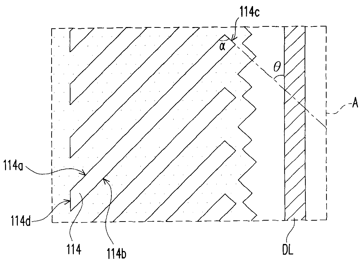
[0086] In this embodiment, each strip electrode 142 has a first end 142a and a second end 142b, each first end 142a is connected to the first main electrode part 120 or the second main electrode part 130, and the same strip electrode group 140 The second ends 142b in each are connected to each other. In more detail, each second end 142b of this embodiment has a branch 142b - 1 , and each branch 142b - 1 is respectively connected to the second end 142b of the adjacent strip electrode 142 . In this embodiment, each branch 142b - 1 can extend in a direction parallel to the data line DL, so ...
experiment example
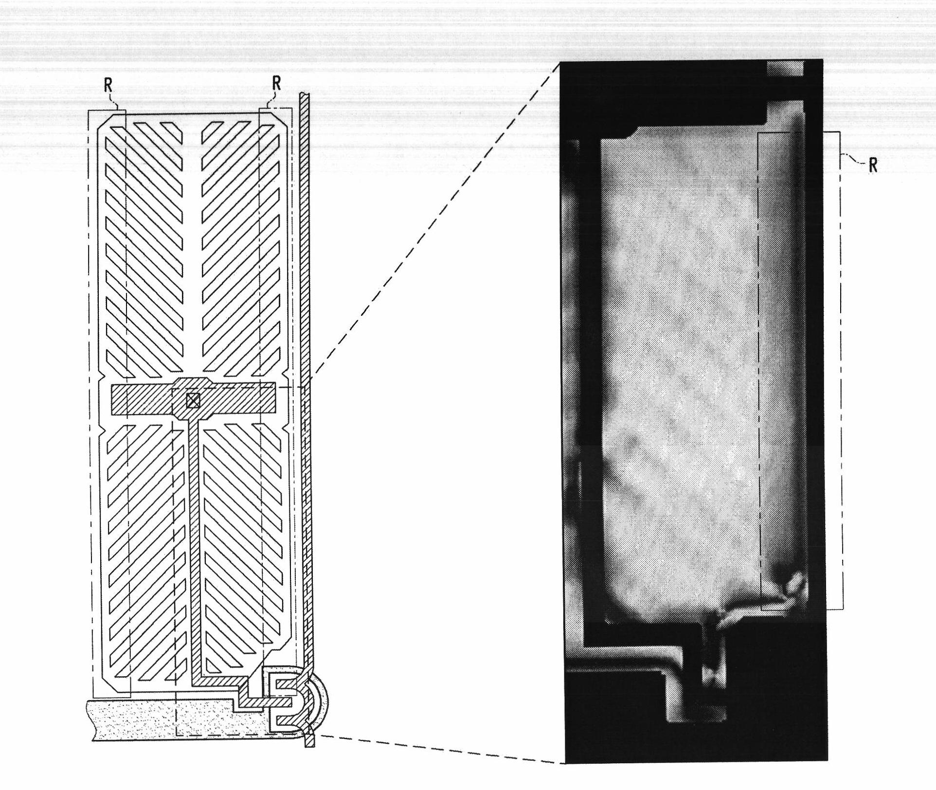
[0089] figure 1 It is a schematic diagram of the existing pixel structure. Figure 8 It is a schematic diagram of a pixel structure 1000 according to the first embodiment of the present invention. Figure 9 It is a schematic diagram of a pixel structure 1000A according to the second embodiment of the present invention. Depend on figure 1 It can be seen that in the existing pixel structure, disclination lines are likely to occur on both sides R of the pixel electrode. Compare figure 1 and Figure 8 It can be seen that the disclination line problem on both sides R of the pixel electrode of the pixel structure 1000 of the first embodiment is improved. Similarly, by Figure 9 The problem of disclination lines on both sides R of the pixel electrode of the pixel structure 1000A shown in the second embodiment is further improved.
[0090] In addition, please refer to Figure 9 and Figure 10 , in the pixel structure 1000A of the second embodiment, the shortest distance between...
PUM
 Abstract
Description
Claims
Application Information