A silicon-based hybrid integrated avalanche photodetector

A photodetector, integrated avalanche technology, applied in circuits, electrical components, semiconductor devices, etc., can solve the problems of low coupling efficiency of couplers, unfavorable on-chip interconnection, mutual restriction of responsivity and bandwidth of surface incident detectors, etc. Effects of improved coupling efficiency and low loss characteristics

Active Publication Date: 2017-07-28
INST OF SEMICONDUCTORS - CHINESE ACAD OF SCI
View PDF4 Cites 0 Cited by
  • Summary
  • Abstract
  • Description
  • Claims
  • Application Information

AI Technical Summary

Problems solved by technology

[0005] The main purpose of the present invention is to provide a high-responsivity, high-bandwidth silicon-based integrated evanescent field coupled waveguide avalanche detector structure to solve the low coupling efficiency of the coupler, mutual constraints between the responsivity and bandwidth of the surface-incidence detector, and inconsistencies. Conducive to issues such as on-chip interconnection

Method used


Image

  • A silicon-based hybrid integrated avalanche photodetector
  • A silicon-based hybrid integrated avalanche photodetector
  • A silicon-based hybrid integrated avalanche photodetector

Examples


Embodiment Construction

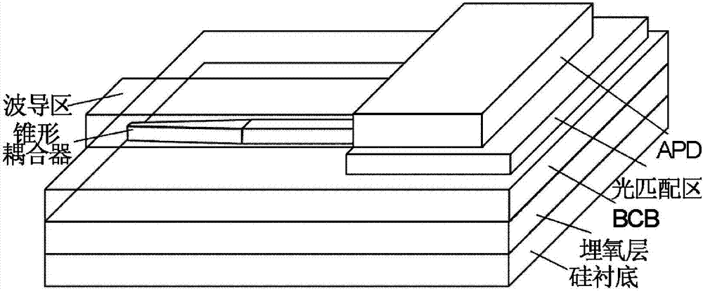
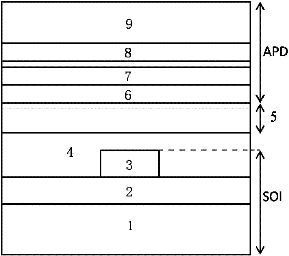
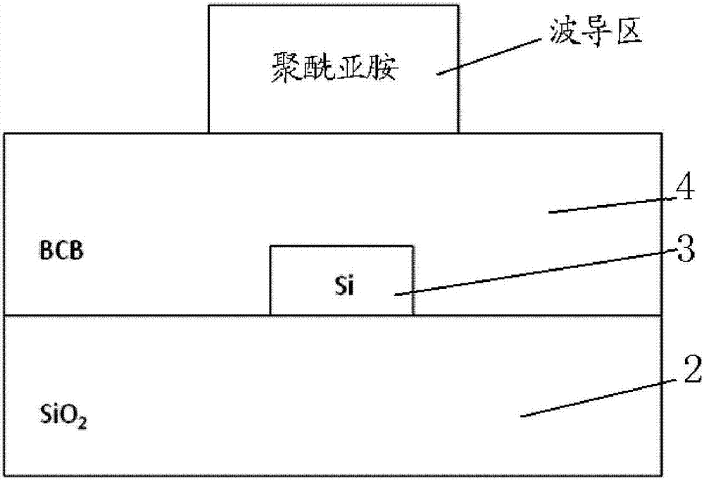
[0034] To solve the aforementioned technical problems, there are two key points: one is the layer structure of SOI inverted tapered coupler, BCB thickness, polymer waveguide region, optical matching region and absorption region, and their size design to achieve stable transmission of light The high-responsivity detection of light can be achieved by the efficient and fast coupling into the absorption region; the second is the optimization of the layer structure and thickness doping of the avalanche photodetector that affects the electrical characteristics, and can obtain low carrier transition Time, low RC constant, and narrow multiplication region, etc., so as to realize high-speed, low-noise photodetection with internal gain.

[0035] In order to realize a high-efficiency integrated photodetector, the present invention proposes an SOI-based tapered coupling APD device, which is expected to be applied to silicon-based photoelectric integrated chips and quantum communications. ...


PUM


Abstract

The invention discloses a silicon-based hybrid integrated avalanche photodetector (APD). The silicon-based hybrid integrated avalanche photodetector comprises an SOI (silicon-on-insulator) inverted cone coupling structure, a bonding layer, a waveguide and optical matching layer and an avalanche photodetecting structure, which are superposed from bottom to top; and the waveguide and optical matching layer comprises a waveguide region and an optical matching region. The silicon-based hybrid integrated avalanche photodetector is built through a bonding technology; the high-efficiency coupling target is achieved by using an inverted cone template conversion coupling structure and an evanescent wave optical coupling way; an APD of a separate absorption charge multiplication region (SACM) can reach the target of high-speed and low-noise optical detection through a narrow multiplication layer and a narrow absorption layer; and the avalanche photodetector simultaneously integrates the advantages of the SOI inverted cone coupling structure and the avalanche photodetecting structure in a manner of bonding the SOI inverted cone coupling structure and the avalanche photodetecting structure.

Description

technical field [0001] The invention relates to the technical field of silicon-based hybrid integrated photodetectors, in particular to an evanescent field coupled avalanche photodetector integrated on SOI. Background technique [0002] In recent years, silicon-based photonics has developed rapidly, and the simultaneous integration of multiple optical active and passive devices on silicon-based chips makes the prospect of silicon-based integration even broader. Photodetectors are important components in photonic systems. In the future, as photonic systems have higher and higher requirements for high bandwidth and high integration, the requirements for detector performance will also be higher. Because the bandwidth and responsivity of traditional surface-incidence detectors are mutually restricted, and the integration of surface-incidence devices and waveguide functional structures is also greatly restricted. Waveguide avalanche detection can satisfy both high responsivity a...

Claims


Application Information

Patent Timeline
Patent Type & Authority Patents(China)
IPC IPC(8): H01L31/107H01L31/0232
CPCH01L31/02325H01L31/1075
Inventor 尹冬冬杨晓红韩勤何婷婷吕倩倩
Owner INST OF SEMICONDUCTORS - CHINESE ACAD OF SCI
Why Eureka
Try Eureka