Anti-ringing circuit

An anti-ringing and circuit technology, applied in the electronic field, can solve problems such as affecting the normal operation of the circuit

Inactive Publication Date: 2016-07-20
UNIV OF ELECTRONICS SCI & TECH OF CHINA
View PDF4 Cites 4 Cited by
  • Summary
  • Abstract
  • Description
  • Claims
  • Application Information

AI Technical Summary

Problems solved by technology

[0002] In the general BUCK type DC-DC converter architecture, such as figure 1 As shown, PCH is the power upper tube, NCH is the synchronous rectification switch tube, and capacitor C is the parasitic capacitance between the drains of PCH and NCH to ground. In CCM mode, the inductor current will not cross zero in the whole cycle, and the capacitor C is at When the synchronous rectifier tube is turned on, it is short-circuited by NCH, and when the power top tube is on, it is short-circuited by the low impedance loop formed by PCH and the power supply, so there will be no oscillation phenomenon. However, in DCM mode, when the circuit crosses zero, the upper and lower tubes are turned off at the same time. There is no low-impedance loop to short-circuit C. Therefore, the parallel connection of the inductance L, the parasitic capacitance C, the load capacitance CL and the load resistance R together constitutes the LC oscillation loop, and the SW terminal will form an obvious high-frequency oscillation. The fundamental wave of these oscillations Harmonics may be coupled to sensitive circuits such as RF through the magnetic field leakage of the inductor or parasitic capacitance, affecting the normal operation of the circuit

Method used


Image

  • Anti-ringing circuit
  • Anti-ringing circuit
  • Anti-ringing circuit

Examples


Embodiment Construction

[0034] Below in conjunction with accompanying drawing, describe technical scheme of the present invention in detail:

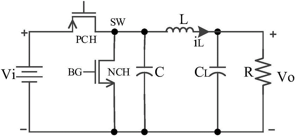
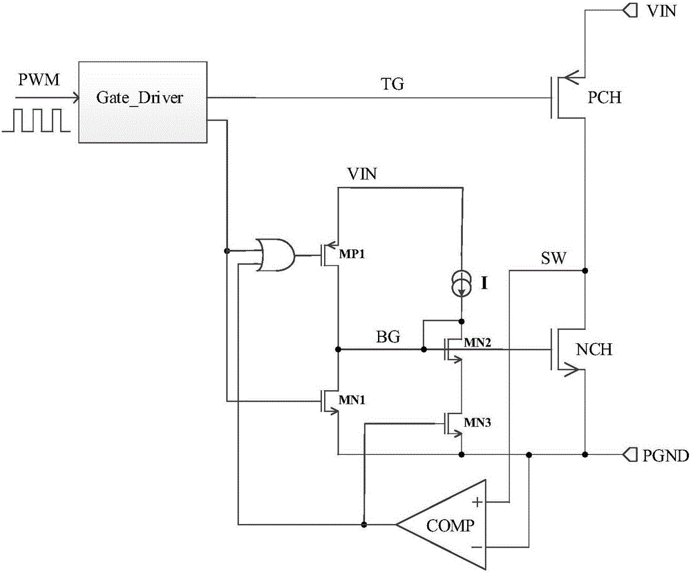
[0035] Such as figure 2 Shown is the connection method between the drive circuit and the gate discharge circuit of the synchronous rectifier. In the light load mode, when BG is high, the synchronous rectifier is turned on. After the system detects the zero crossing, the output of the zero crossing comparator jumps high. The OR gate shielding loop makes the transistor MP1 cut off, the gate signal of the synchronous rectifier is floating, and the switch tube MN3 is turned on at the same time, so that MN2 and the synchronous rectifier form a current mirror structure. At this time, the synchronous rectifier controls the SW point with a certain current. The release of energy reduces the SW ringing phenomenon.

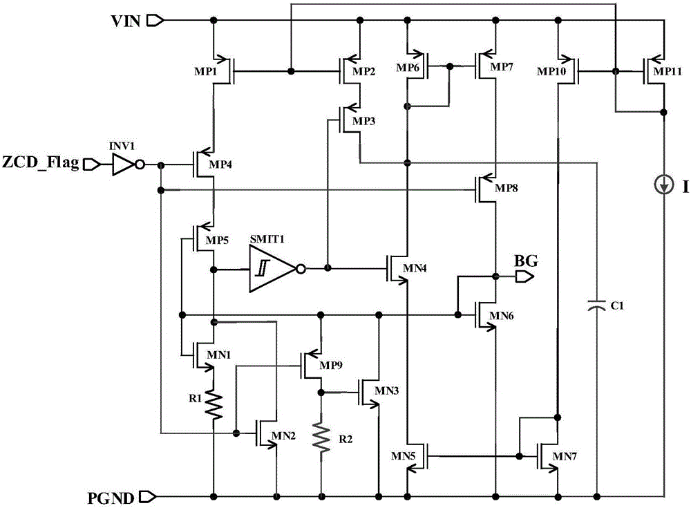
[0036] The specific implementation of the synchronous rectifier gate discharge circuit is shown in the figure image 3 Shown:

[0037] The principle is:...


PUM


Abstract

The present invention belongs to the field of the electronic technology, and specifically relates to an anti-ringing circuit. A synchronization rectifier tube grid discharging circuit is employed, after a circuit is zero crossing, the synchronization rectifier tube is not closed immediately, and the synchronization rectifier tube grid rapidly discharges to a low potential to perform weak conduction, when the voltages at two ends of the inductor is equal, the synchronization rectifier tube is thoroughly turned off, and the circuit is located at a stable state, the voltage of a SW is equal to the output voltage without oscillation, therefore the anti-ringing effect is reached.

Description

technical field [0001] The invention belongs to the field of electronic technology, and in particular relates to an anti-ringing circuit. Background technique [0002] In the general BUCK type DC-DC converter architecture, such as figure 1 As shown, PCH is the power upper tube, NCH is the synchronous rectification switch tube, and capacitor C is the parasitic capacitance between the drains of PCH and NCH to ground. In CCM mode, the inductor current will not cross zero in the whole cycle, and the capacitor C is at When the synchronous rectifier tube is turned on, it is short-circuited by NCH, and when the power top tube is on, it is short-circuited by the low impedance loop formed by PCH and the power supply, so there will be no oscillation phenomenon. However, in DCM mode, when the circuit crosses zero, the upper and lower tubes are turned off at the same time. There is no low-impedance loop to short-circuit C. Therefore, the parallel connection of the inductance L, the par...

Claims


Application Information

Patent Timeline
Patent Type & Authority Applications(China)
IPC IPC(8): H02M1/44
CPCH02M1/44
Inventor 周泽坤何烨李要张波
Owner UNIV OF ELECTRONICS SCI & TECH OF CHINA
Why Eureka
Try Eureka