
Method for manufacturing ceramic part with closed cavity structure for high-frequency high-speed ceramic package shell

A technology of ceramic packaging and manufacturing method, which is applied in semiconductor/solid-state device manufacturing, electrical components, electrical solid-state devices, etc. Effect

Active Publication Date: 2016-07-27
THE 13TH RES INST OF CHINA ELECTRONICS TECH GRP CORP
View PDF3 Cites 15 Cited by
  • Summary
  • Abstract
  • Description
  • Claims
  • Application Information

AI Technical Summary

Problems solved by technology

Relying on the traditional multi-layer ceramic shell processing technology, a narrower wiring width of the internal RF lines of the ceramic is required, and the screen printing process used for the internal lines is due to its own process characteristics - screen mesh, metal paste and printing processing It is difficult to meet the design requirements of ceramic shells with higher frequencies and speeds due to constraints such as manufacturability

Method used


Image

  • Method for manufacturing ceramic part with closed cavity structure for high-frequency high-speed ceramic package shell
  • Method for manufacturing ceramic part with closed cavity structure for high-frequency high-speed ceramic package shell

Examples


Embodiment Construction

[0023] The technical solutions in the embodiments of the present invention are clearly and completely described below in conjunction with the accompanying drawings in the embodiments of the present invention. Obviously, the described embodiments are only part of the embodiments of the present invention, not all of them. Based on the embodiments of the present invention, all other embodiments obtained by persons of ordinary skill in the art without making creative efforts belong to the protection scope of the present invention.

[0024] In the following description, a lot of specific details are set forth in order to fully understand the present invention, but the present invention can also be implemented in other ways different from those described here, and those skilled in the art can do it without departing from the meaning of the present invention. By analogy, the present invention is therefore not limited to the specific examples disclosed below.

[0025] Such as figure ...

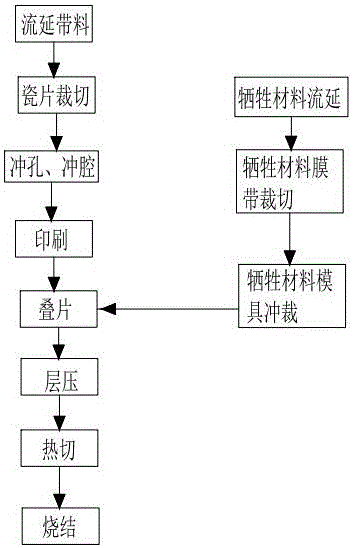
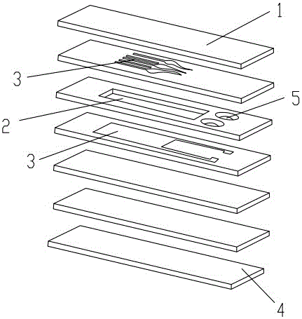

PUM


Abstract

The invention discloses a method for manufacturing a closed-cavity ceramic part for a high-frequency and high-speed ceramic packaging shell, and relates to the technical field of semiconductor microelectronic device preparation. The method comprises the following steps: preparing a green porcelain tape; using a punching device to punch holes and form a cavity on the cut green porcelain tape at a position where holes need to be punched and forming a cavity; The required metallization pattern is printed by screen printing on the corresponding position of the side wall; the sacrificial material is filled inside the formed cavity; the laminated green ceramic sheet is laminated, and the interlayer density is controlled by adjusting the process parameters and the shape of the cavity; sintering the prepared green porcelain piece, during the sintering process of the green porcelain piece, the sacrificial material is burnt out, and a ceramic piece with a closed cavity structure is prepared. The inside of the closed cavity of the ceramic part prepared by the method has a good shape, and the wiring on the bottom side of the closed cavity can meet the higher frequency signal transmission requirements.

Description

technical field [0001] The invention relates to the technical field of semiconductor microelectronic device preparation, in particular to a method for manufacturing a closed-cavity structural ceramic part for a high-frequency, high-speed ceramic packaging shell. Background technique [0002] The ceramic parts are alumina ceramics, but not limited to alumina ceramics, aluminum nitride ceramics, LTCC and other ceramics. The traditional multi-layer ceramic processing adopts tape casting process to prepare green ceramic strips, which are cut into standard-sized green ceramic sheets, and punching equipment is used to process positioning holes and cavities on the green ceramic sheets, and tungsten paste is used on the surface of the green ceramic sheets material or molybdenum paste, gold, silver, copper and other conductive pastes can also be used, metallized graphics are printed by precision screen printing technology, multi-layer raw ceramic sheets are stacked, laminated, and th...

Claims


Application Information

Patent Timeline
IPC IPC(8): H01L21/48H01L23/053
CPCH01L21/4807H01L23/053
Inventor 郑欣刘林杰吴亚光丁飞任才华陈军伟张义政白洪波
Owner THE 13TH RES INST OF CHINA ELECTRONICS TECH GRP CORP
Learn More