Method and apparatus for non-contact measurement of internal quantum efficiency in light emitting diode structures

A technology for light-emitting diodes and luminescence measurement, which is used in diode testing, measuring devices, electrical excitation analysis, etc., and can solve problems such as high contact resistance, difficult alignment measurement artifacts, blocked electroluminescence, and inability to consider lateral currents.

Active Publication Date: 2016-08-03
KLA TENCOR TECH CORP
View PDF12 Cites 5 Cited by
  • Summary
  • Abstract
  • Description
  • Claims
  • Application Information

AI Technical Summary

Problems solved by technology

One of the main disadvantages of this technique is that the electroluminescence close to the contact area of ​​the probe is blocked by the probe itself and thus only the peripheral and scattered part of the luminescent signal is collected
In addition, another disadvantage of this technique includes the inability to account for lateral currents in the p-n junction layer, which can cause a significant spread of electroluminescence outside the electrode area, leading to a significant contribution to measurement errors
Furthermore, this method suffers from the presence of measurement artifacts related to contamination, high contact resistance, alignment difficulties, presence of particles and the like

Method used


Image

  • Method and apparatus for non-contact measurement of internal quantum efficiency in light emitting diode structures
  • Method and apparatus for non-contact measurement of internal quantum efficiency in light emitting diode structures
  • Method and apparatus for non-contact measurement of internal quantum efficiency in light emitting diode structures

Examples


Embodiment Construction

[0039] Reference will now be made in detail to the disclosed subject matter, which is illustrated in the accompanying drawings.

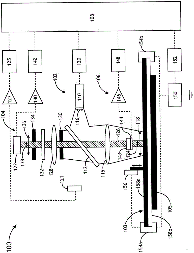
[0040] generally refer to Figures 1A to 4C , describe systems and methods for non-contact measurement of one or more characteristics of light emitting diode (LED) structures in accordance with the present invention. Embodiments of the invention relate to a luminescence measurement technique suitable for measuring electroluminescence (EL) responses and / or photoluminescence (PL) responses from LED structures illuminated by excitation illumination. In addition, embodiments of the present invention relate to a non-contact junction photovoltage ( JPV) technology.

[0041] The non-contact measurement techniques described throughout this disclosure provide accurate measurements of one or more characteristics of LED structures. In some embodiments, the non-contact measurement techniques of the present invention can provide, but are not limited to, monit...


PUM


Abstract

Non-contact measurement of one or more electrical response characteristics of a LED structure includes illuminating an illumination area of a surface of a light emitting diode structure with one or more light pulses, measuring a transient of a luminescence signal from a luminescence area within the illumination area of the light emitting diode structure with a luminescence sensor, determining a first luminescence intensity at a first time of the measured transient of the luminescence signal from the light emitting diode structure, determining a second luminescence intensity at a second time different from the first time of the measured transient of the luminescence signal from the light emitting diode structure and determining an intensity of the electroluminescence component of the luminescence signal from the light emitting diode structure based on the first luminescence signal and the second luminescence signal.

Description

[0001] Cross References to Related Applications [0002] This application asserts rights under 35 U.S.C. §119(e) to U.S. Provisional Application No. 61 / 877,949, filed September 14, 2013, and U.S. Provisional Application No. 61 / 933,284, filed January 29, 2014 . US Provisional Application No. 61 / 877,949 and US Provisional Application No. 61 / 933,284 are hereby incorporated by reference in their entirety. technical field [0003] The present invention relates generally to the non-contact measurement of various electrical response characteristics in light emitting diode structures, and in particular, the present invention relates to a non-contact technique for measuring the internal quantum efficiency of light emitting diode structures. Background technique [0004] The need for improved semiconductor device characterization techniques has increased along with the ever-increasing demand for improved semiconductor device performance. Semiconductor wafers, such as silicon wafers...

Claims


Application Information

Patent Timeline
Patent Type & Authority Applications(China)
IPC IPC(8): G01R31/26
CPCG01R31/2635G01N21/66G01N2033/0095G01N33/00
Inventor V·N·法伊费尔
Owner KLA TENCOR TECH CORP
Why Eureka
Try Eureka