
White-light scanning interferometry measurement method and system

A technology of white light scanning and interferometry, applied in measuring devices, optical devices, instruments, etc., can solve problems such as large errors, and achieve wide application and strong anti-noise performance

Active Publication Date: 2016-08-17
SOUTH CHINA NORMAL UNIVERSITY
View PDF6 Cites 13 Cited by
  • Summary
  • Abstract
  • Description
  • Claims
  • Application Information

AI Technical Summary

Problems solved by technology

White light phase-shift interferometry refers to the operation method of single-wavelength phase-shifting. This method is suitable for processing objects with smooth surfaces, and it will cause large errors when the phase-shift interval is not selected accurately.
[0005] The above-mentioned white light scanning interference zero optical path difference positioning methods all have their own limitations and have a certain scope of application.

Method used


Image

  • White-light scanning interferometry measurement method and system
  • White-light scanning interferometry measurement method and system
  • White-light scanning interferometry measurement method and system

Examples


no. 1 example

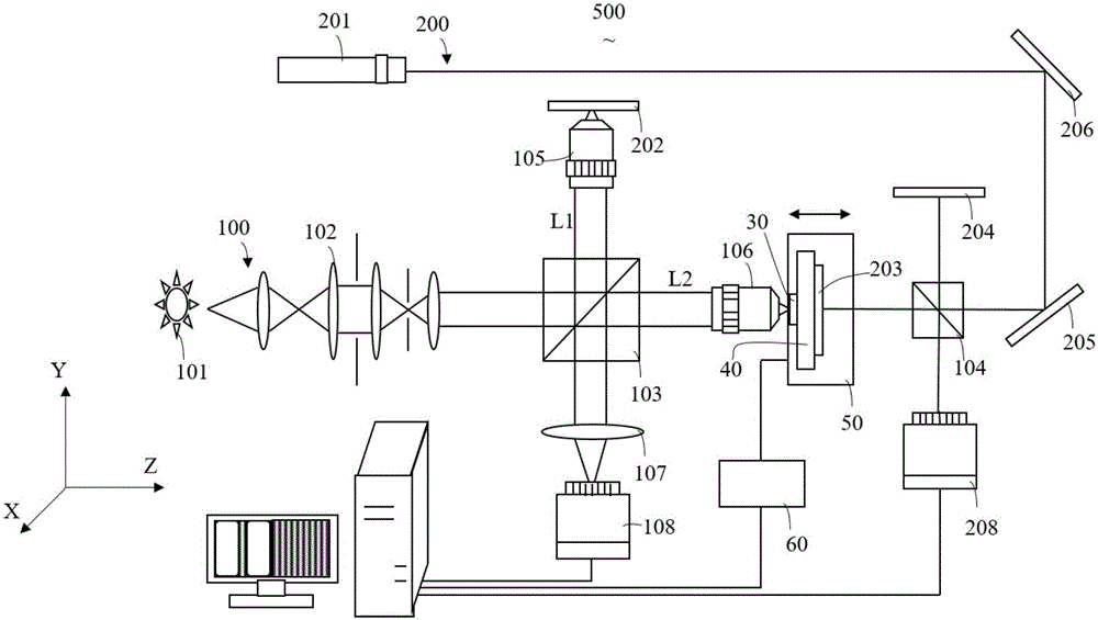
[0015] Such as figure 1 As shown, the white light scanning interferometry system 500 provided by the first embodiment of the present invention includes a white light scanning module 100, a calibration module 200, a fixed plate 40 for fixing the object to be measured 30, a piezoelectric ceramic micro-displacement platform 50, and a piezoelectric ceramic micro-displacement platform 50. Electroceramic controller 60.

[0016] Wherein said white light scanning module 100 comprises: a white light source 101, a Koehler illumination system 102, a first beam splitter 103 and a second beam splitter 104, a first microscope objective lens 105 and a second microscope An objective lens 106 , an imaging lens 107 , and a first monochromatic black and white image sensor 108 .

[0017] Wherein the calibration module 200 includes a laser 201; a first plane mirror 202, a second plane mirror 203, a third plane mirror 204, a fourth plane mirror 205, a fifth plane mirror 206, a second single color...

no. 2 example

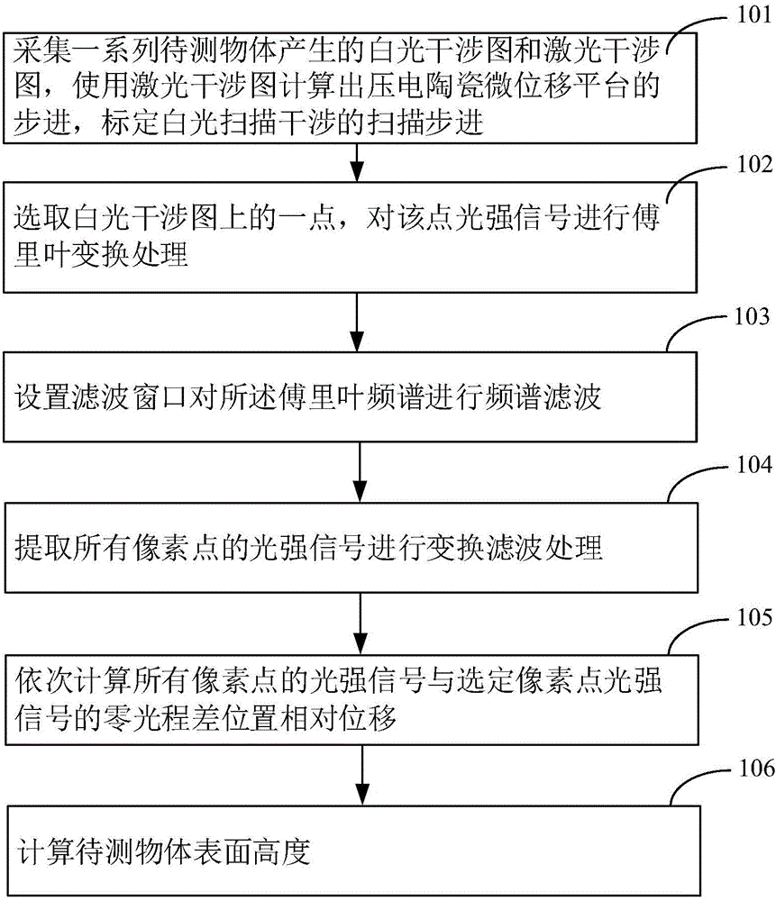
[0034] Please refer to figure 2 , the white light scanning interferometry method based on generalized correlation time delay estimation will be further described in conjunction with the accompanying drawings and embodiments in conjunction with this embodiment. In this method, the white light scanning interferometry system 500 described in the first embodiment is used to perform The measurement includes the following steps S101-S106.

[0035] Step S101, collect a series of white light interferograms and laser interferograms generated by the object to be measured, use the laser interferogram to calculate the step of the piezoelectric ceramic micro-displacement platform 50, and calibrate the scanning step of the white light scanning interference:

[0036] During specific measurement, a computer is used to drive the first monochrome black-and-white image sensor 108 and the second monochrome black-and-white image sensor 208 to simultaneously collect a series of white light interfe...


PUM

PropertyMeasurementUnit
Wavelengthaaaaaaaaaa

Abstract

The invention relates to a white-light scanning interferometry measurement method and system. The system comprises a white-light scanning module, a calibration module, a fixed flat plate and a piezoelectric ceramic micro displacement platform, wherein the white-light scanning module comprises a white light source, a Kohler illumination system, a first beam splitter, a second beam splitter, a first microobjective, a second microobjective, an imaging lens, first, second, third, fourth and fifth plane mirrors and a first single-color black-and-white image sensor; the calibration module comprises a laser and a second single-color black-and-white image sensor. According to the system and the method, the central wavelength of a light source is not required to be calibrated, the calculation accuracy is not affected by enveloping shapes of interference signals, the anti-noise performance is good, and the method and the system can be widely applied to signal processing of white-light scanning interferometry measurement.

Description

technical field [0001] The invention relates to the field of white light scanning interference three-dimensional shape measurement, in particular to a white light scanning interferometry method and system based on generalized correlation time delay estimation. Background technique [0002] As a three-dimensional shape measurement method, white light scanning interferometry is widely used in the three-dimensional shape measurement of microscopic objects and the surface roughness measurement of objects. With the development of precision manufacturing, it is necessary to measure the three-dimensional shape of some MEMS devices, semiconductor chips and other objects whose surface height jumps from hundreds of nanometers to hundreds of microns. Currently used probe-type measurement methods such as atomic force microscopes and spherometers have certain limitations and are not suitable for the three-dimensional shape measurement of such objects. [0003] Moreover, the white light ...

Claims


Application Information

Patent Timeline
IPC IPC(8): G01B11/24
CPCG01B11/2441
Inventor 吕晓旭蔡红志周云飞刘胜德钟丽云
Owner SOUTH CHINA NORMAL UNIVERSITY
Learn More