
Electronic component device production method and electronic component sealing sheet

A technology for electronic components and manufacturing methods, which is applied in semiconductor/solid-state device manufacturing, electrical components, electronic equipment, etc., can solve problems such as inability to position and align, and achieve the effect of suppressing pollution

Inactive Publication Date: 2016-08-17
NITTO DENKO CORP
View PDF1 Cites 5 Cited by
  • Summary
  • Abstract
  • Description
  • Claims
  • Application Information

AI Technical Summary

Problems solved by technology

As a result, there is a problem that the alignment cannot be performed again

Method used


Image

  • Electronic component device production method and electronic component sealing sheet
  • Electronic component device production method and electronic component sealing sheet
  • Electronic component device production method and electronic component sealing sheet

Examples


Embodiment 1~3 and comparative example 1

[0218] According to the compounding ratio described in Table 1, compound the ingredients, and use a roll mill to heat the mixture under reduced pressure (0.01kg / cm2) at 60-120°C for 10 minutes. 2 ) were melt-kneaded to prepare a kneaded product. Next, the obtained kneaded product was arranged so as to be sandwiched between two 50 μm protective films (manufactured by Mitsubishi Plastics Corporation: trade name "MRF"), and the kneaded product was formed into a sheet by a flat press method to produce A sheet for sealing with a thickness of 200 μm.

Embodiment 4

[0220] According to the compounding ratio described in Table 1, the epoxy resin, phenolic resin, thermoplastic resin and inorganic filler were added into the organic solvent MEK (methyl ethyl ketone) in a manner that the solid content concentration was 95%, and stirred. Stirring was performed at 800 rpm for 5 minutes using a planetary mixer (manufactured by Thinky Co., Ltd.). Thereafter, according to the compounding ratio described in Table 1, carbon black and a curing accelerator were further compounded, and MEK was added so that the solid content concentration became 90%, and further stirred at 800 rpm for 3 minutes to obtain a coating liquid.

[0221] Thereafter, the coating solution was coated on a silicone release-treated polyethylene terephthalate film having a thickness of 50 μm, and dried at 120° C. for 3 minutes to prepare a resin sheet with a thickness of 100 μm. Furthermore, the produced resin sheet was bonded together at 90 degreeC with the roll laminator, and the ...


PUM

PropertyMeasurementUnit
forceaaaaaaaaaa
thicknessaaaaaaaaaa
softening pointaaaaaaaaaa

Abstract

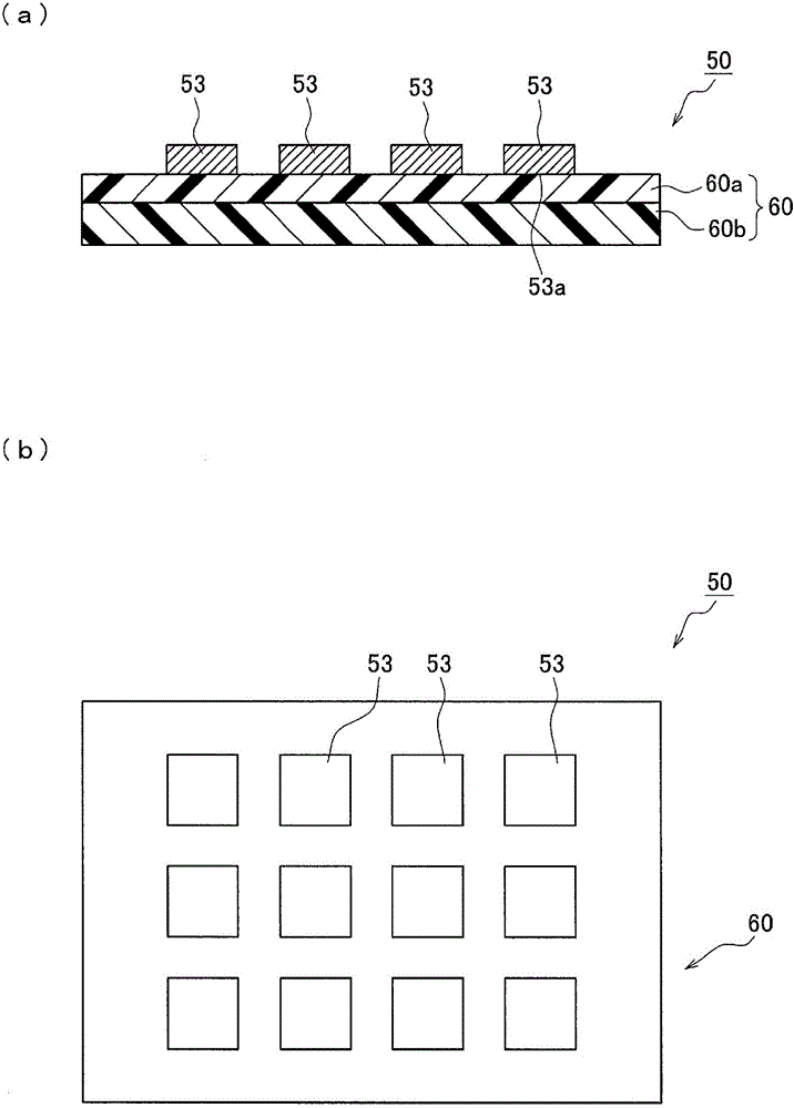
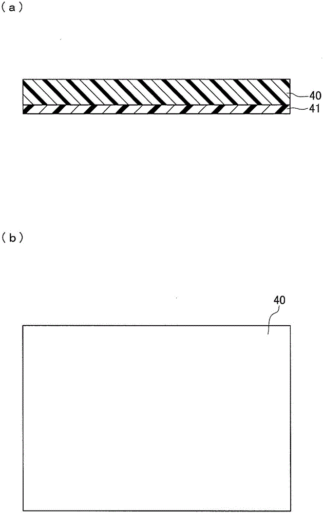
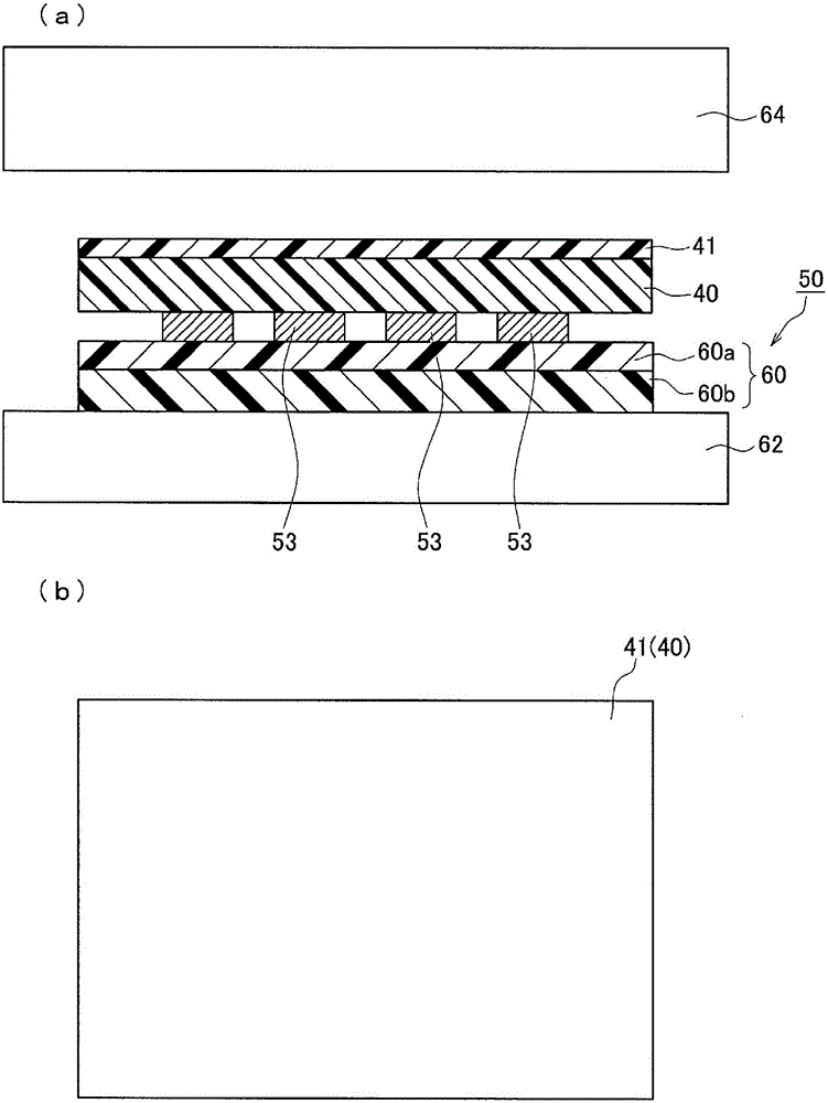
The electronic component device production method includes a step A of preparing a layered body comprising electronic components immobilized on a support body, a step B of preparing an electronic component sealing sheet, a step C of disposing the electronic component sealing sheet over the electronic components under conditions where the probe tack force of the electronic component sealing sheet is 5 gf or lower according to a probe tack test, a step D of rising the temperature of the electronic component sealing sheet until the probe tack of the electronic component sealing sheet is 10 gf or greater according to the probe tack test to immobilize temporarily the electronic component sealing sheet onto the electronic components, and a step E of embedding the electronic components in the electronic component sealing sheet to form a sealed body comprising the electronic components embedded in the electronic component sealing sheet.

Description

technical field [0001] The present invention relates to a manufacturing method of an electronic component device and a sheet for electronic component sealing. Background technique [0002] Conventionally, as a method of manufacturing a semiconductor device, there is known a method of sealing one or a plurality of semiconductor chips fixed on a substrate or the like with a sealing resin, and then dicing the sealed body into packages of semiconductor device units. As such sealing resin, the sheet|seat for sealing which consists of thermosetting resin is known, for example (for example, refer patent document 1). [0003] prior art literature [0004] patent documents [0005] Patent Document 1: Japanese Patent Laid-Open No. 2006-19714 Contents of the invention [0006] The problem to be solved by the invention [0007] When manufacturing an electronic component device by the above-mentioned method, it is necessary to align and arrange the sealing sheet so that it is locat...

Claims


Application Information

Patent Timeline
Patent Type & Authority Applications(China)
IPC IPC(8): H01L21/56C09K3/10H01L23/29H01L23/31
CPCB32B3/08B32B5/18B32B5/20B32B7/12B32B15/046B32B15/06B32B25/08B32B25/12B32B27/065B32B27/26B32B27/38B32B27/42B32B37/182B32B37/185B32B37/187B32B2255/10B32B2255/26B32B2307/51B32B2307/536B32B2309/02B32B2309/04B32B2309/105B32B2367/00B32B2457/14H01L21/56H01L21/561H01L21/568H01L23/3107H01L24/19H01L24/96H01L24/97H01L2224/12105H01L2924/181H01L2924/18162H01L2924/00C09K3/10H01L23/29H01L23/31B29C65/02B29K2667/003B29L2031/3481B32B7/10B32B27/08B32B27/36B32B37/06B32B2307/20C08J5/18C08J2363/02C08J2433/10C08J2461/06H01L21/78H01L23/293H01L24/13H01L2924/0665
Inventor 志贺豪士石坂刚盛田浩介饭野智绘
Owner NITTO DENKO CORP
Learn More