Processing apparatus

A technology for processing devices and processed objects, which is applied in the direction of electrical components, semiconductor/solid-state device manufacturing, circuits, etc., can solve problems such as time-consuming, and achieve the effect of reducing axis movement

Inactive Publication Date: 2016-08-31
DISCO CORP
View PDF7 Cites 2 Cited by
  • Summary
  • Abstract
  • Description
  • Claims
  • Application Information

AI Technical Summary

Problems solved by technology

[0007] However, in this case, in addition to the cost for installing the two microscopes, initial settings (settings such as alignment and focus positions) and maintenance for each microscope are required.
In addition, in order to obtain an image at a desired magnification, it is necessary to move the axis to position the microscope at the imaging position, and it takes time to perform the positioning.

Method used


Image

  • Processing apparatus
  • Processing apparatus
  • Processing apparatus

Examples


no. 1 Embodiment approach

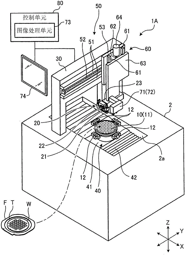
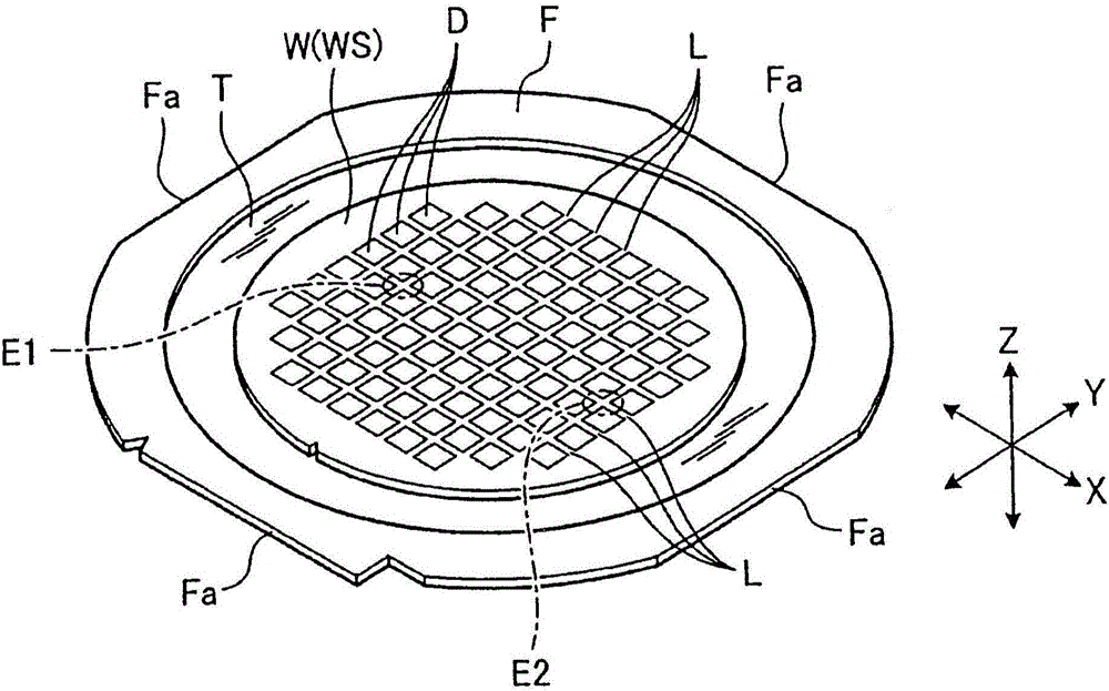
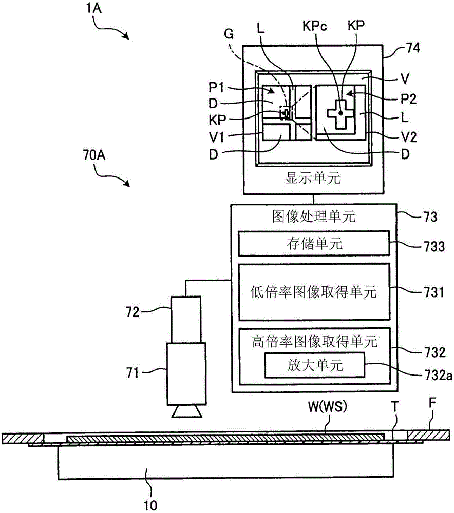
[0023] Next, a configuration example of the processing device according to the first embodiment will be described. figure 1 It is a perspective view which shows the structural example of the processing apparatus of 1st Embodiment. figure 2 It is a perspective view showing the imaging area of ​​the wafer according to the first embodiment. image 3 It is a block diagram showing a configuration example of the calibration unit of the first embodiment.

[0024] The processing apparatus 1A is used to cut the wafer W. As shown in FIG. The processing device 1A has a chuck table 10 , a processing unit 20 , a portal frame 30 , a processing feed unit 40 , an index feed unit 50 , a plunging feed unit 60 , a calibration unit 70A, and a control unit 80 .

[0025] The wafer W is various workpieces such as semiconductor wafers and optical device wafers formed with semiconductor devices and optical devices, inorganic material substrates, ductile resin material substrates, ceramic substrates...

no. 2 Embodiment approach

[0049] Next, a processing device according to a second embodiment will be described. Figure 5 It is a block diagram showing a configuration example of the calibration unit of the second embodiment. Figure 5 The illustrated calibration unit 70B differs from the calibration unit 70A of the first embodiment in that the low-magnification image acquisition unit 731 includes an image compression unit 731 a.

[0050] The image compression unit 731a compresses the low-magnification image data, for example, using methods such as JPEG (Joint Photograph Experts Group: Joint Photographic Experts Group) or GIF (Graphics Interchange Format: Graphics Interchange Format) to compress the low-magnification image data to about a fraction .

[0051] Next, an example of the operation of the calibration unit 70B will be described. Figure 6 It is a flowchart showing an operation example of the calibration unit of the second embodiment. In this example, as a premise of the description, the notc...


PUM


Abstract

The invention provides a processing apparatus which simplifies the structure of a calibration device. The processing apparatus processes an image which is photographed by one optical system (71) and an image photographing unit (72), thereby obtaining a low-magnification image (P1) and a high-magnification image (P2). Therefore, in acquiring the low-magnification image (P1) and the low-magnification image (P2), arrangement of an optical system (71) and an image photographing unit (72) for high magnificiation and an optical system (71) and an image photographing unit (72) for low magnification are not required, thereby reducing cost of the optical system (71) and the image photographing unit (72) and reducing maintenance cost of the optical system (71) and the image photographing unit (72). Furthermore, in acquiring the low-magnification image (P1) and the high-magnification image (P2), positioning for shaft motion of the optical system (71) can be finished through one-time operation, thereby reduucing number of shaft motions.

Description

technical field [0001] The present invention relates to processing devices and in particular to calibration units. Background technique [0002] Processing using cutting equipment, laser processing equipment, etc. for the purpose of dividing various plate-shaped workpieces such as semiconductor wafers, wafers on which optical devices are formed, package substrates on which electronic components are formed, ceramic substrates, and glass substrates, etc. device. The processing device uses the imaging unit to image the key patterns formed on the front and rear surfaces of the workpiece held on the chuck table, and estimates the area to be processed (planned dividing line) using the key patterns as clues. An imaging unit for imaging a key pattern conventionally includes a low-magnification macroscopic microscope and a high-magnification microscopic microscope. The macroscopic microscope detects the key pattern, and the microscopic microscope accurately estimates the position of...

Claims


Application Information

Patent Timeline
Patent Type & Authority Applications(China)
IPC IPC(8): H01L21/68
CPCH01L21/681H01L21/682
Inventor 赤濑胜彦寺师健太郎
Owner DISCO CORP
Why Eureka
Try Eureka