Supercharge Your Innovation With Domain-Expert AI Agents!

A low-power rectifier component using ball planting technology and its manufacturing method

A manufacturing method and component technology, applied in semiconductor/solid-state device manufacturing, electrical components, electrical solid-state devices, etc., can solve the problems of difficult processing, high cost of production raw materials, unstable quality, etc., and achieve good electrical and thermal conductivity , Reduce the cost of raw materials and improve production efficiency

Active Publication Date: 2018-09-04
SHANDONG JINGDAO MICROELECTRONICS
View PDF4 Cites 0 Cited by
  • Summary
  • Abstract
  • Description
  • Claims
  • Application Information

AI Technical Summary

Problems solved by technology

Although copper wires and silver wires have appeared in recent years, the current production process capacity cannot provide copper wires and silver wires below 1mil
Moreover, gold is a rare and precious metal. The welding process of gold wire not only has high production raw material costs, but also relatively low production process efficiency.
[0004] Lead frame stacking and jumper welding processes, such as: SOD123, MB, UMB, etc., due to the limitations of the lead frame stamping manufacturing process, the plane (boss plane or bending plane) that is in contact with the positive electrode of the chip, its length and width or diameter The size should not be less than 0.3mm, otherwise, the processing will be very difficult and the quality will be very unstable. Therefore, manufacturers using lead frame stacking and chip jumper welding processes cannot produce high-quality, high-yield products with small-size chips below 30mil×30mil
For a 30mil×30mil chip, the length and width of the effective positive soldering area are very close to 0.3mm. If the length and width or diameter of the plane in contact with the positive pole of the chip is 0.3mm, then the plane of the lead frame that is in contact with the chip can easily touch the chip The protective layer on the edge seriously affects the quality of semiconductor components
Compared with the metal wire welding process, although the production equipment of the lead frame stacking and jumper welding process is relatively simple and the production efficiency is high, it is difficult to produce small-sized chip diodes and rectifier bridge semiconductor devices, which means that almost all low-power diodes use wire The reason for the welding process

Method used


Image

  • A low-power rectifier component using ball planting technology and its manufacturing method
  • A low-power rectifier component using ball planting technology and its manufacturing method
  • A low-power rectifier component using ball planting technology and its manufacturing method

Examples


Embodiment 1

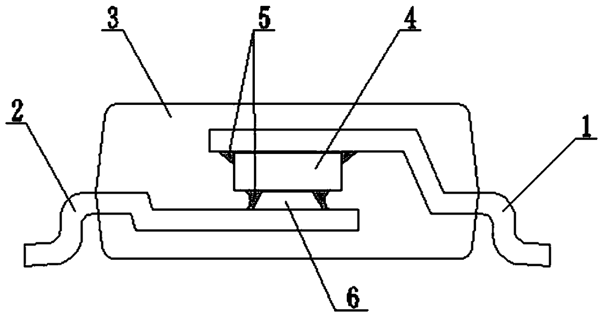
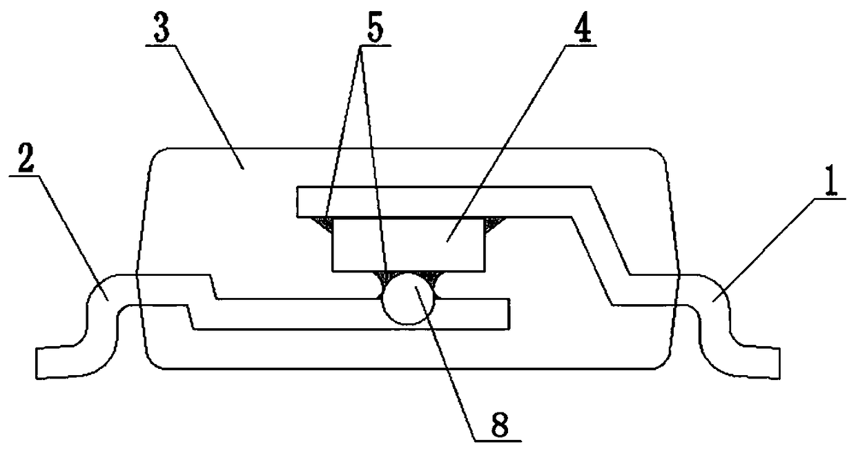
[0038] Such as image 3 As shown, the present invention adopts the low-power rectifying components of the ball planting process, including a plastic-encapsulated epoxy resin 3, which is provided with a lead frame A 1 and a lead frame B 2 located below the lead frame A; the lead frame A The lower surface of 1 is welded with chip 4 and the positive electrode of the chip is facing downward. On the upper surface of lead frame B 2 and corresponding to the position of the chip, a spherical crown pit or through hole 22 is set to fix the conductive ball 8. The conductive ball 8 and the chip 4 The positive poles are in contact to form a current path.

Embodiment 2

[0040] A kind of manufacturing method of low-power rectifying component and parts as described in embodiment 1, comprises steps as follows:

[0041] S1, fixing the chip: Dip and coat solder 5 on the chip welding surface 11 where all lead frames A 1 and the chip are welded, such as Figure 4 As shown, the solder 5 adopts solder paste; the chip 4 is placed on the chip soldering surface 11 coated with solder, with the positive electrode of the chip facing up, as Figure 5 As shown, the chip 4 is fixed on the lead frame A1.

[0042] S2, ball planting:

[0043] Before planting the ball, process the ball crown pit or through hole 22 on the conductive ball soldering surface 21 of the lead frame B2 to fix the conductive ball, such as Figure 7 shown;

[0044] On the conductive ball soldering surface 21 of all lead frames B 2, dip and coat solder 5 or flux, such as Figure 6 As shown, the solder 5 adopts solder paste;

[0045] Manufacture a stencil matching the lead frame B2, the ...


PUM


Abstract

The invention discloses a small-power rectification component adopting a ball-embedding process and a manufacturing method thereof. The rectification component comprises plastic packaging epoxy resin. A lead frame A and a lead frame B arranged below the lead frame A are arranged in the plastic packaging epoxy resin. A chip is welded to the lower surface of the lead frame A, and the positive electrode of the chip is downward. A conductive ball is arranged on the position, corresponding to the chip, on the surface of the lead frame B. The conductive ball is in contact with the positive electrode point of the chip so as to form a current path. According to the invention, the welding process of the conductive call is adopted, the conductive path is shorter, welding is more reliable, the electricity conduction and heat conduction performance is better, and the quality of the product is improved; the expensive gold wires are not used any more, so that the cost of the raw material is substantially lowered; in addition, the embedded conductive ball and the chip are in point contact, the chip very small in size can be produced, the ball-embedding process is simple and mature, and compared with the metal wire welding process, the production efficiency is improved by about 8 times.

Description

technical field [0001] The invention relates to a low-power rectifying component and a manufacturing method using a ball-planting process, and belongs to the technical field of semiconductor devices. Background technique [0002] Low-power diodes and rectifier bridge semiconductor components, such as: SOD123, SOD323, MB, and ABS, etc., generally have the following three welding connection methods between the positive electrode of the chip and the pin: 1. Metal wire welding connection, such as figure 2 2. The connection method of lead frame overlay welding, such as figure 1 As shown, the lead frame in contact with the positive electrode of the chip usually has a convex plane formed by extrusion or a bending plane formed by bending, and the plane projection shape is generally a regular quadrilateral or a circle; 3. Jumper (Clip ) Welding connection method, there is also a plane part on the jumper that is in contact with the positive electrode of the chip, and its formation m...

Claims


Application Information

Patent Timeline
Patent Type & Authority Patents(China)
IPC IPC(8): H01L23/495H01L21/60
CPCH01L23/49517H01L23/49537H01L24/80H01L2224/80H01L2224/16245H01L2224/32245H01L2224/33181H01L2224/48091H01L2224/48465H01L2224/73253H01L2224/73265H01L2224/97H01L2924/181H01L2924/00014H01L2924/00012
Inventor 朱坤恒孔凡伟段花山
Owner SHANDONG JINGDAO MICROELECTRONICS
Features
  • R&D
  • Intellectual Property
  • Life Sciences
  • Materials
  • Tech Scout
  • Unparalleled Data Quality
  • Higher Quality Content
  • 60% Fewer Hallucinations
Learn More