High voltage jfet device and process method

A process method and device technology, applied in the field of high-voltage JFET devices, can solve problems such as concentration drop, and achieve the effects of reducing pinch-off voltage, simple implementation, and improving breakdown voltage

Active Publication Date: 2019-10-11
SHANGHAI HUAHONG GRACE SEMICON MFG CORP
View PDF2 Cites 0 Cited by
  • Summary
  • Abstract
  • Description
  • Claims
  • Application Information

AI Technical Summary

Problems solved by technology

The measured pinch-off voltage is only 40V, because the P-well 104 as the gate of the JFET is all located under the field oxygen 103, and its concentration is lower than that of the P-well under the active region.

Method used


Image

  • High voltage jfet device and process method
  • High voltage jfet device and process method
  • High voltage jfet device and process method

Examples


Embodiment Construction

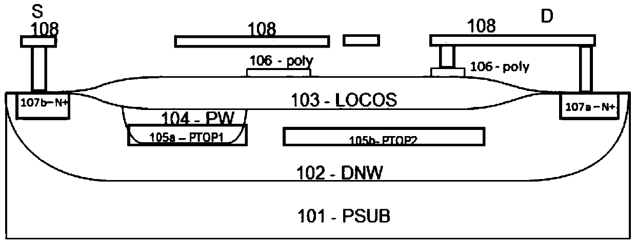
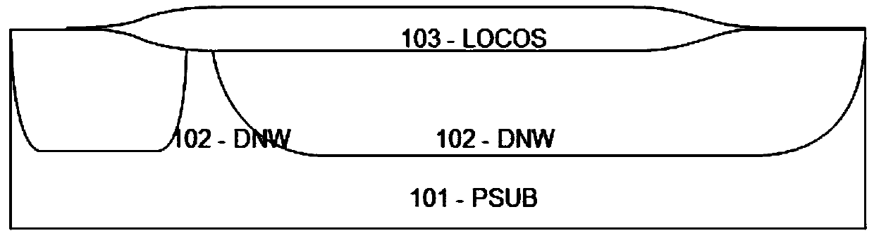
[0026] High voltage JFET device described in the present invention, such as Figure 8 As shown, there is an N-type deep well 102 in the P-type substrate 101. From the cross-sectional perspective, the field oxygen 103 is above the N-type deep well 102, and the two ends of the field oxygen 103 are the source region 107b and the drain region of the JFET respectively. 107 a , the field oxygen 103 covers the polysilicon field plate 106 .

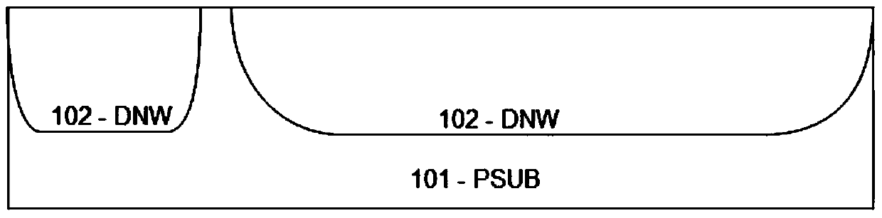
[0027] The N-type deep well 102 is divided into two sections, the first N-type deep well and the second N-type deep well, such as Figure 8 As shown in , the first N-type deep well 102 on the left side includes the source region 107b of the JFET, and the second N-type deep well 102 on the right side includes the drain region 107a of the JFET and the P-type injection layer 105b; the first The N-type deep well and the second N-type deep well are independent of each other, with a certain distance between them, generally 2-6 μm, and the distance can...


PUM


Abstract

The invention discloses a high voltage JFET device and a processing method of the same. A P substrate is provided with a deep N-well. From a cutaway view angle, a field oxide is on the deep N-well, and the two ends of the field oxide are a JFET source area and a drain area. The field oxide is covered with a poly-silicon field plate. The deep N-well is divided into two sections: a first deep N-well section and a second deep N-well section wherein the first deep N-well section contains the JFET source area and the second deep N-well section contains the JFET drain area and a P injection layer. The first deep N-well section and the second deep N-well section are independent from each other. Between the first deep N-well section and the second deep N-well section is a P-well. The P-well shares the sizes with both the two deep N-well sections. Also between the first deep N-well section and the second deep N-well section is the P injection layer. The P injection layer, right under the P well, also shares sizes with with both the two deep N-well sections. The JFET device provided by the invention is provided with adjustable pinch-off voltage and at the same time, with high breakdown voltage as well. The invention also discloses a processing method for such a high voltage JFET device.

Description

technical field [0001] The invention relates to a semiconductor device, in particular to a high-voltage JFET device. The invention also relates to the process method of the high-voltage JFET device. Background technique [0002] LDMOS with a withstand voltage of 500V not only has the characteristics of high voltage and high current of discrete devices, but also absorbs the advantages of high-density intelligent logic control of low-voltage integrated circuits. A single chip can realize the functions that can only be completed by multiple chips, which greatly reduces the area, reduces the cost, and improves It meets the development direction of miniaturization, intelligence and low energy consumption of modern power electronic devices. The 500V JFET mounted on this platform is an important device of the drive circuit, and its breakdown voltage is particularly important as a key parameter to measure the 500V JFET. [0003] A conventional 500V JFET device structure such as f...

Claims


Application Information

Patent Timeline
Patent Type & Authority Patents(China)
IPC IPC(8): H01L29/808H01L29/06H01L21/337
Inventor 段文婷
Owner SHANGHAI HUAHONG GRACE SEMICON MFG CORP
Why Eureka
Try Eureka