Liquid crystal display panel and manufacturing method thereof as well as display device

A technology for a liquid crystal display panel and a manufacturing method, which is applied in nonlinear optics, instruments, optics, etc., can solve the problems of light leakage, scratched PI film, position shift, etc. The effect of force, contact area density reduction

Inactive Publication Date: 2016-09-07
BOE TECH GRP CO LTD
View PDF5 Cites 23 Cited by
  • Summary
  • Abstract
  • Description
  • Claims
  • Application Information

AI Technical Summary

Problems solved by technology

However, when the liquid crystal display panel is subjected to an external force, the position of the top of the main PS (the end in contact with the array substrate) may be displaced, and in severe cases, it will be displaced into the pixel area, which will scratch the PI film in the pixel area. In turn, it may cause light leakage or blue spots on the LCD panel.

Method used


Image

  • Liquid crystal display panel and manufacturing method thereof as well as display device
  • Liquid crystal display panel and manufacturing method thereof as well as display device
  • Liquid crystal display panel and manufacturing method thereof as well as display device

Examples


Embodiment 1

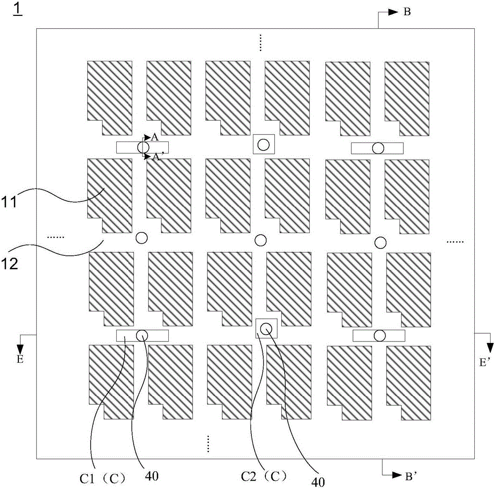
[0038] The embodiment of the present invention is mainly aimed at the problem that the top of the columnar spacer (PS) in the liquid crystal display panel is prone to position displacement, which may cause light leakage or blue spot phenomenon. Therefore, the liquid crystal display panel of the embodiment of the present invention should include PS . Generally speaking, a liquid crystal display panel is formed by two substrates paired with a cell, and the PS is located between the two substrates to ensure a certain cell thickness between the two substrates. PS has a bottom end and a top end; since the PS is set on one of the substrates, one end of the PS set on the substrate is called the bottom end of the PS, the bottom end of the PS is fixed, and the other end of the PS is called the top end of the PS. The top of the PS will abut against the upper surface of another substrate, and the top of the PS may be displaced.

[0039] Next, the structure of the liquid crystal display ...

Embodiment 2

[0072] An embodiment of the present invention provides a display device, which may include any liquid crystal display panel 1 provided in Embodiment 1, so the display device is also called a liquid crystal display device. Exemplarily, the liquid crystal display device may include other components such as a backlight module and a frame in addition to the liquid crystal display panel 1 .

[0073] The liquid crystal display device may be a product or component with any display function, such as a liquid crystal display, a liquid crystal TV, a digital camera, a mobile phone, and a tablet computer. In the display device provided by the embodiment of the present invention, by adding spacer limiting groove C, the top of the columnar spacer can be placed in the groove, thereby restricting the movement of the top of the spacer; The limit groove C is located in the pixel boundary area 12, thereby reducing the positional displacement of the top of the columnar spacer to the pixel area; i...

Embodiment 3

[0075] An embodiment of the present invention provides a method for manufacturing a liquid crystal display panel. The liquid crystal display panel includes a pixel area and a pixel defining area surrounding the pixel area. refer to Figure 10 , the manufacturing method includes the following steps:

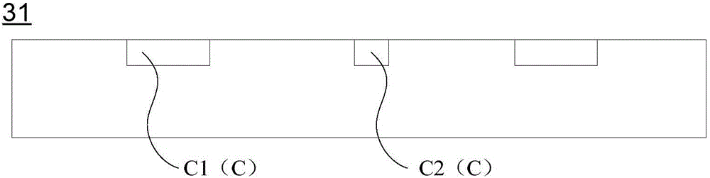
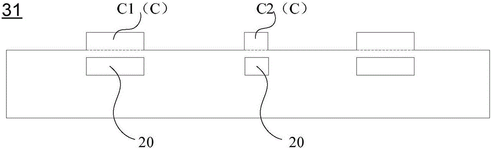
[0076] S101 , forming a thin film on the first substrate, and patterning the part of the thin film located in the pixel defining region to form a groove, so as to obtain the first substrate 31 with a spacer limiting groove C on the upper surface.

[0077] The material of the first substrate can be glass or flexible material.

[0078] Wherein, those skilled in the art can select the material for making the thin film according to actual needs, for example, metals, such as molybdenum, copper, silver, etc. can be selected. Taking the first substrate 31 as an array substrate and fabricating spacer support pads with grooves on the flat layer as an example, this step can specifically b...


PUM


Abstract

The embodiment of the invention discloses a liquid crystal display panel and a manufacturing method thereof as well as a display device, and relates to the technical field of display, so as to solve the problem that pixel region position offset easily occurs to the top end of a columnar spacer. The liquid crystal display panel is provided with a pixel region and a pixel definition region surrounding the pixel region; the liquid crystal display panel comprises a first substrate and a second substrate which are oppositely arranged; in the pixel definition region, the upper surface of the first substrate is provided with a spacer limiting slot; the second substrate is provided with a columnar spacer; the top end of the columnar spacer props against the spacer limiting slot of the first substrate; under a condition that the liquid display panel is in the absence of external force, a clearance is reserved between the top end of the spacer and the bottom end of the spacer limiting slot.

Description

technical field [0001] The invention relates to the field of display technology, in particular to a liquid crystal display panel, a manufacturing method thereof, and a display device. Background technique [0002] A liquid crystal display panel is usually formed by aligning an array substrate and a color filter substrate and injecting liquid crystal between the two substrates. In the manufacturing process of a liquid crystal display panel, the distance between the array substrate and the color filter substrate is a very important quality factor. [0003] In order to maintain the gap (Cell Gap, cell thickness) between the array substrate and the color filter substrate, it is mainly used to add a certain thickness of spacer (Spacer) between the two substrates before the cell is aligned to maintain the cell thickness. Commonly used spacers mainly include two types: Ball Spacer (BS for short) and Post Spacer (PS for short). If BS is used to manufacture liquid crystal display pa...

Claims


Application Information

Patent Timeline
Patent Type & Authority Applications(China)
IPC IPC(8): G02F1/1339G02F1/1333
CPCG02F1/13394G02F1/1333
Inventor 贾倩
Owner BOE TECH GRP CO LTD
Why Eureka
Try Eureka