Array substrate manufacturing method, array substrate and display device

A manufacturing method and array substrate technology, applied in semiconductor/solid-state device manufacturing, electrical components, electrical solid-state devices, etc., to achieve the effects of improving negative bias stress tolerance, maintaining tolerance, and ensuring reliability

Inactive Publication Date: 2016-09-21
BOE TECH GRP CO LTD
View PDF5 Cites 3 Cited by
  • Summary
  • Abstract
  • Description
  • Claims
  • Application Information

AI Technical Summary

Problems solved by technology

[0004] In order to solve the problem of how to ensure the reliability of the oxide thin film transistors in the display area, an e

Method used


Image

  • Array substrate manufacturing method, array substrate and display device
  • Array substrate manufacturing method, array substrate and display device
  • Array substrate manufacturing method, array substrate and display device

Examples


Example Embodiment

[0044] In order to make the object, technical solution and advantages of the present invention clearer, the implementation manner of the present invention will be further described in detail below in conjunction with the accompanying drawings.

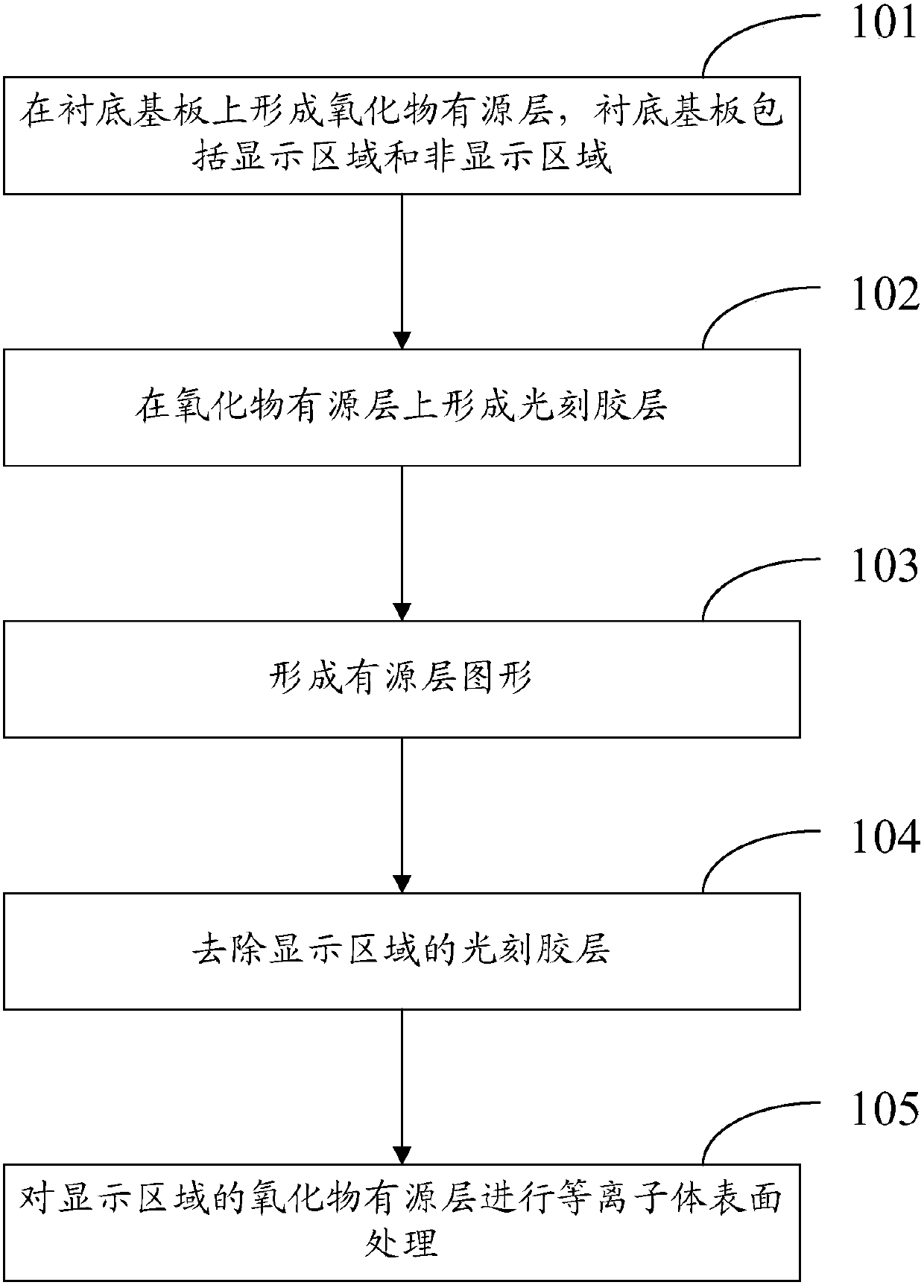
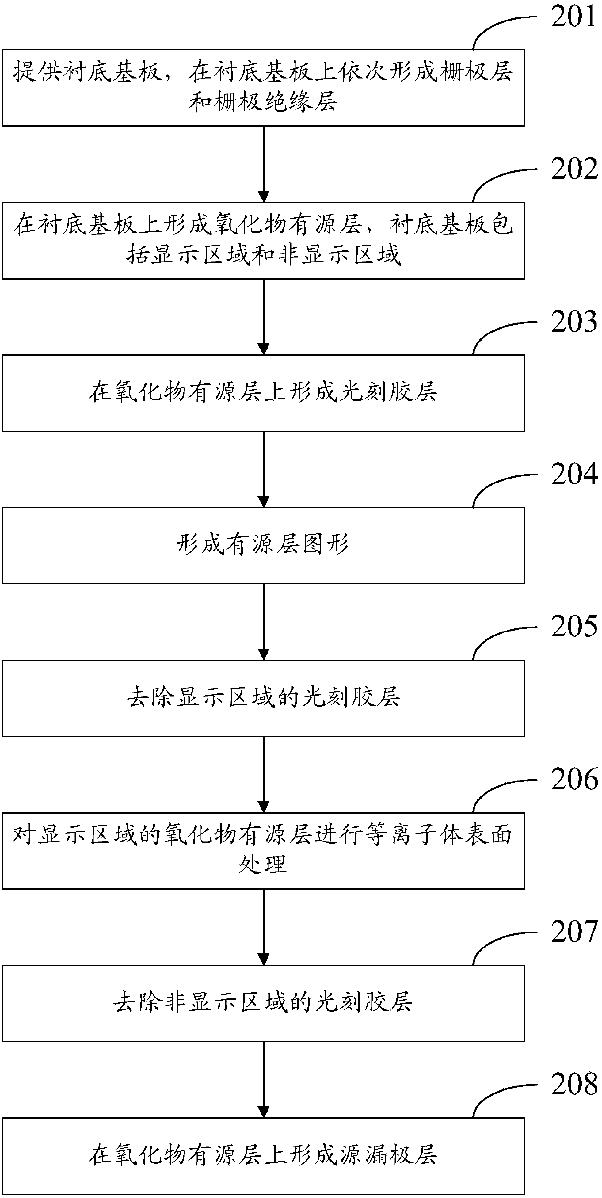
[0045] see figure 1 , an embodiment of the present invention provides a manufacturing method of an array substrate, the manufacturing method comprising:

[0046] Step 101 : forming an oxide active layer on a base substrate, where the base substrate includes a display area and a non-display area.

[0047] Step 102: forming a photoresist layer on the oxide active layer.

[0048] Step 103: forming an active layer pattern.

[0049] Step 104: removing the photoresist layer in the display area.

[0050] Step 105: performing plasma surface treatment on the oxide active layer in the display area, so as to increase the oxygen content in the oxide active layer in the display area.

[0051] When performing plasma surface treatment on the oxid...


PUM


Abstract

The invention discloses an array substrate manufacturing method, an array substrate and a display device, belonging to the technical field of display. The manufacturing method comprises steps: forming an oxide active layer on an underlayment substrate, wherein the underlayment substrate comprises a display region and a non-display region; forming a photoresist layer on the oxide active layer; forming an active layer pattern; removing the photoresist layer of the display region; performing plasma surface treatment for the oxide active layer of the display region to increase oxygen content of the oxide active layer of the display region. According to the invention, reliability of thin film transistors of the display region and the non-display region can be guaranteed at the same time.

Description

technical field [0001] The invention belongs to the field of display technology, and in particular relates to a manufacturing method of an array substrate, an array substrate and a display device. Background technique [0002] The gate driver on array (GOA) technology is a process technology for integrating a gate driver circuit on an array substrate. There is an array substrate based on GOA technology. The array substrate includes a display area and a non-display area, and both the display area and the non-display area are realized by oxide thin film transistors (Oxide Thin Film Transistor, Oxide TFT). In the array substrate, the oxide thin film transistors in the display area and the oxide thin film transistors in the non-display area are usually manufactured synchronously by the same process, thereby saving the manufacturing cost of the array substrate and improving the manufacturing efficiency. [0003] During the working process of the array substrate, the oxide thin f...

Claims


Application Information

Patent Timeline
IPC IPC(8): H01L27/12H01L21/77
CPCH01L27/1225H01L27/1259H01L27/127H01L27/1222H01L21/77H01L29/7869
Inventor 崔承镇
Owner BOE TECH GRP CO LTD
Why Eureka
Try Eureka