Manufacturing method for groove grid super junction MOSFET

A manufacturing method and technology of trench gates, which are applied in semiconductor/solid-state device manufacturing, electrical components, circuits, etc., can solve problems such as the influence of the lateral size of the accumulation area, the deterioration of the device's turn-on voltage and conduction voltage drop, and achieve the elimination of sleeve The problem of alignment deviation and the effect of preventing alignment deviation

Active Publication Date: 2016-09-21
SHANGHAI HUAHONG GRACE SEMICON MFG CORP
View PDF4 Cites 2 Cited by
  • Summary
  • Abstract
  • Description
  • Claims
  • Application Information

AI Technical Summary

Problems solved by technology

[0013] figure 2 Although the trench gate structure shown can reduce the size of the device, in the actual process, whether the P-type pillar 3 is formed by multi-layer epitaxy or epitaxial filling, because the P-type pillar 3 and the trench gate, that is, the polysilicon gate 6, are two Sub-photolithography formation, the registration deviation in the process will lead to the situation that the P-type pillar 3 affects the accumula

Method used


Image

  • Manufacturing method for groove grid super junction MOSFET
  • Manufacturing method for groove grid super junction MOSFET
  • Manufacturing method for groove grid super junction MOSFET

Examples


Embodiment Construction

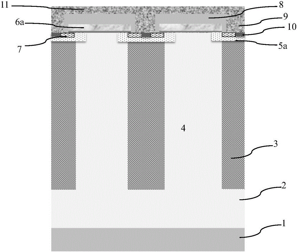
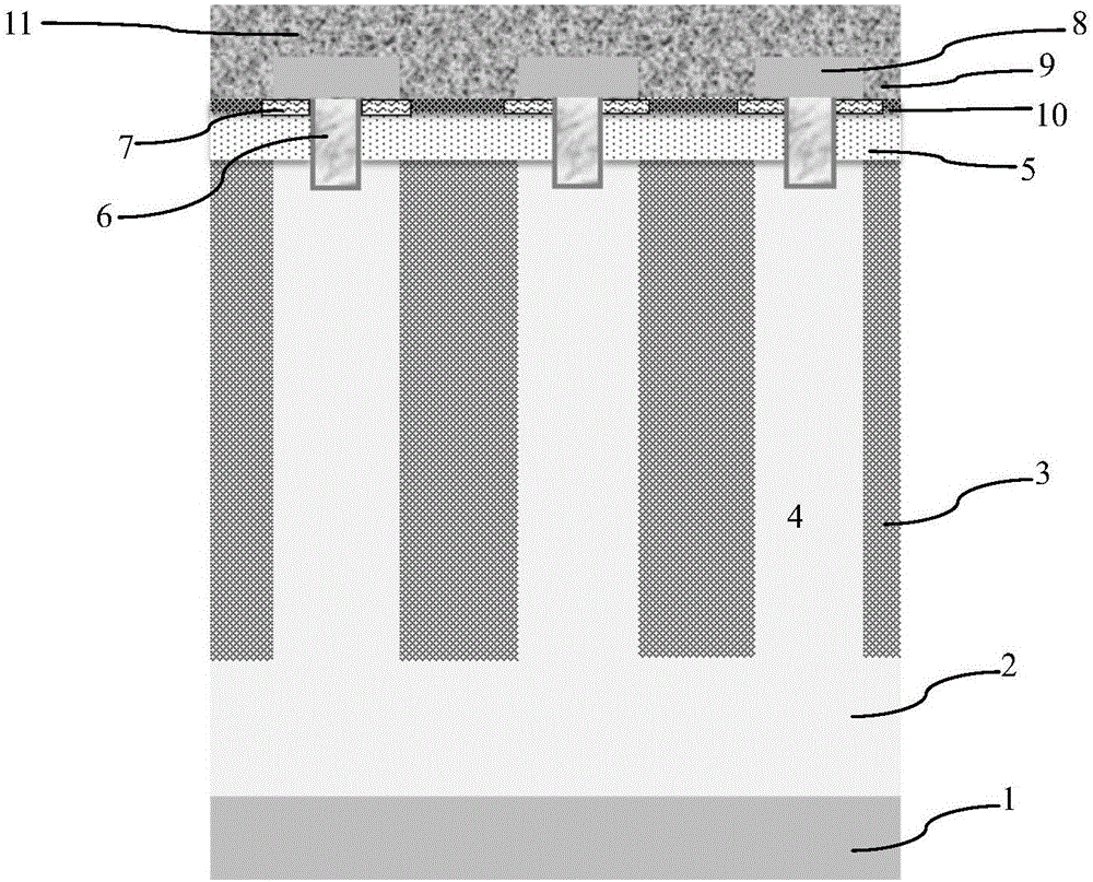
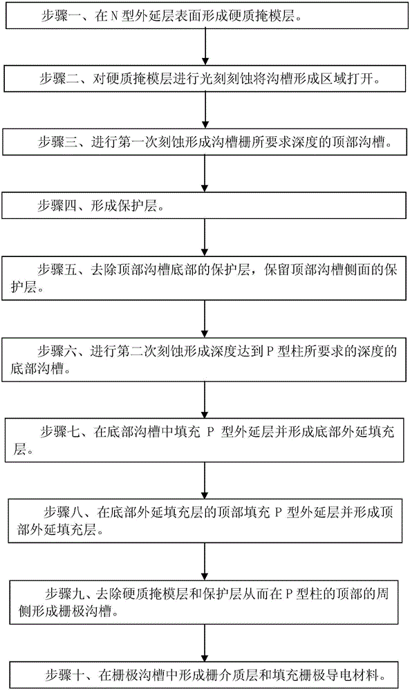
[0045] Such as image 3 Shown is the flow chart of the manufacturing method of the trench gate super junction MOSFET in the embodiment of the present invention; as Figure 4A to Figure 4M As shown, it is a schematic diagram of the device structure in each step of the manufacturing method of the trench-gate super-junction MOSFET according to the embodiment of the present invention. The manufacturing method of the trench-gate super-junction MOSFET according to the embodiment of the present invention includes the following steps:

[0046] Step 1, such as Figure 4A As shown, a semiconductor substrate 101 is provided, and an N-type epitaxial layer 102 is formed on the surface of the semiconductor substrate 101 .

[0047] Such as Figure 4B As shown, a hard mask layer 201 is formed on the surface of the N-type epitaxial layer 102 .

[0048] Preferably, the semiconductor substrate 101 is a silicon substrate, the N-type epitaxial layer 102 is an N-type silicon epitaxial layer, and...


PUM


Abstract

The invention discloses a manufacturing method for a groove grid super junction MOSFET. The manufacturing method comprises the steps of forming a hard mask layer; photoetching the hard mask layer to open a groove forming area; etching for the first time to form a top groove; removing a protection layer at the bottom of the top groove, and reserving the protection layer on the side surface of the top groove; etching for the second time to form a bottom groove; filling the bottom groove with a P-type epitaxial layer to form a bottom epitaxial filled layer; filling the top of the bottom epitaxial filled layer with a P-type epitaxial layer to form a top epitaxial filled layer; removing the hard mask layer and the protection layer and thus forming a grid groove at the periphery of the top of a P-shaped column; and forming a grid dielectric layer in the grid groove and filling a grid conductive material in the grid groove. According to the manufacturing method, the registration deviation between the groove grid and the P-type column can be avoided, the technological stability can be improved and thereby the threshold voltage and breakover voltage drop of the device are more uniform, the size of the super junction unit can be smaller, and the capability of resisting unclamped inductive switching impact can be greatly enhanced.

Description

technical field [0001] The invention relates to a method for manufacturing a semiconductor integrated circuit, in particular to a method for manufacturing a trench gate superjunction (superjunction) power device. Background technique [0002] The super junction structure is composed of alternately arranged N-type pillars and P-type pillars. If the superjunction structure is used to replace the N-type drift region in the vertical double-diffused MOS transistor (Vertical Double-diffused Metal-Oxide-Semiconductor, VDMOS) device, the conduction path is provided through the N-type column in the conduction state, and when the conduction The P-type column does not provide a conduction path; in the off state, the PN column jointly bears the reverse bias voltage, forming a super-junction metal-oxide-semiconductor field-effect transistor (Metal-Oxide-Semiconductor Field-Effect Transistor, MOSFET). The super-junction MOSFET can greatly reduce the on-resistance of the device by using a...

Claims


Application Information

Patent Timeline
IPC IPC(8): H01L29/78H01L21/336H01L29/423H01L29/06
CPCH01L29/0603H01L29/0684H01L29/401H01L29/4236H01L29/66666H01L29/78
Inventor 柯行飞
Owner SHANGHAI HUAHONG GRACE SEMICON MFG CORP
Why Eureka
Try Eureka