

A package structure for optoelectronic integrated chip
A packaging structure and integrated chip technology, applied in the direction of circuits, electrical components, electrical solid devices, etc., can solve problems affecting the transmission and reflection characteristics of devices, and achieve the effects of reducing the impact, avoiding the use of gold wires, and good impedance matching
- Summary
- Abstract
- Description
- Claims
- Application Information
AI Technical Summary
Problems solved by technology
Method used
Image

Examples
Embodiment Construction
[0026] In order to make the object, technical solution and advantages of the present invention clearer, the present invention will be further described in detail below in conjunction with specific embodiments and with reference to the accompanying drawings.
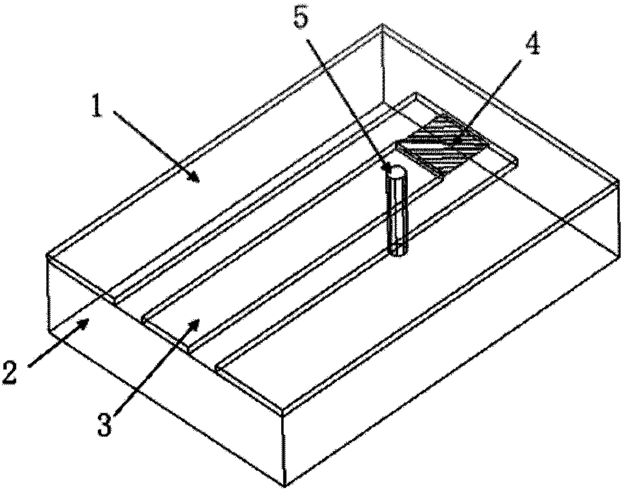
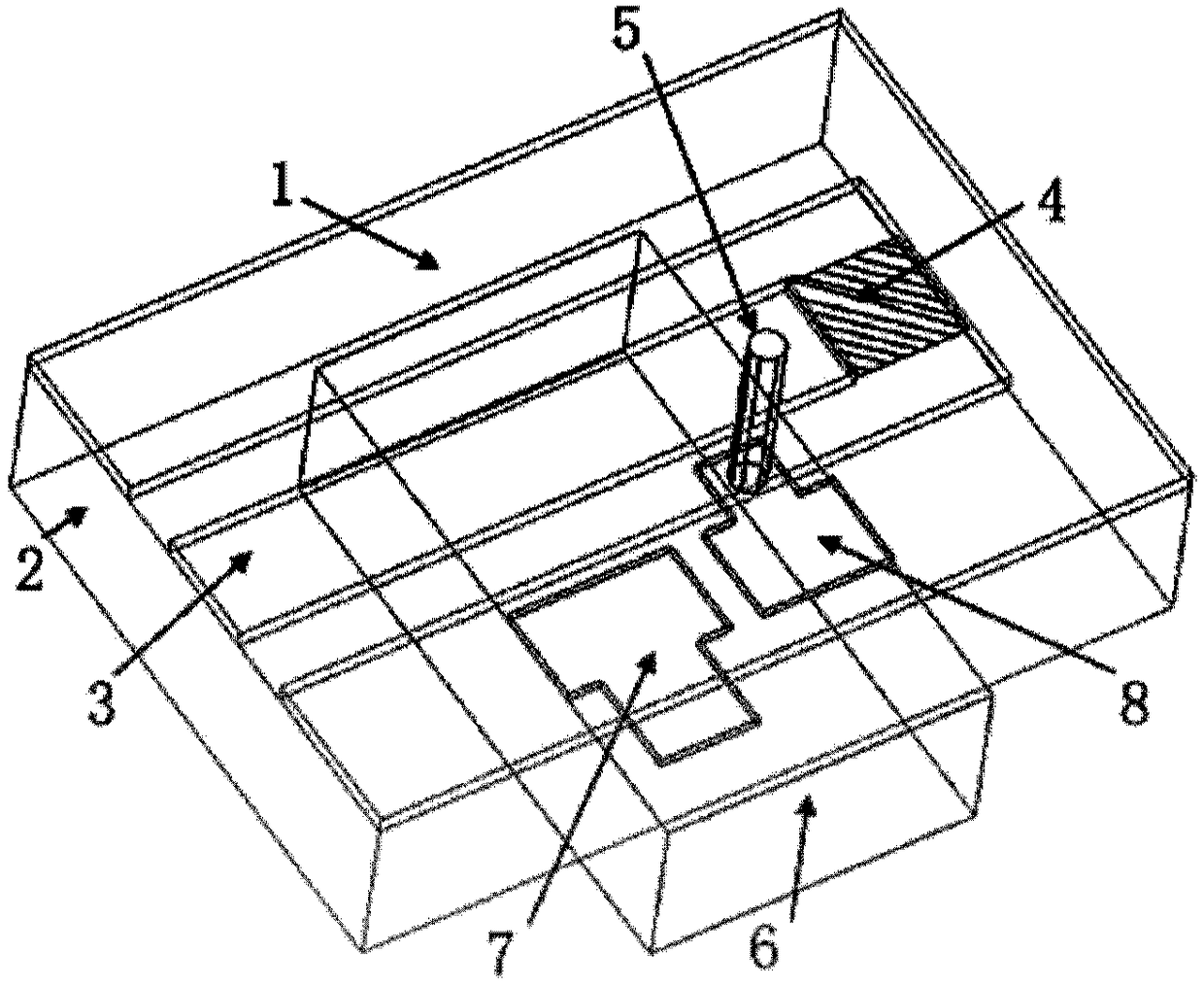
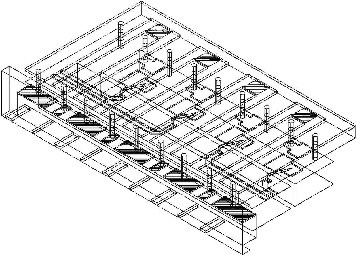
[0027] The invention discloses a packaging structure for an optoelectronic integrated chip, comprising:
[0028] A dielectric substrate, which mainly plays the role of supporting the surface electrodes and confining the electromagnetic field; the surface of the dielectric substrate is evaporated with a certain thickness of coplanar waveguide electrodes by thin film technology, that is, the ground electrode G, the signal electrode S, and the thin film resistance;
[0029] A metal via post, mainly used for signal transmission, connecting signal electrodes and chip electrodes, and supporting dielectric substrate; it can be made by via hole and filling process;
[0030] A matching resistor, connected in parallel with the chip...
PUM
 Abstract
Description
Claims
Application Information