Unlock instant, AI-driven research and patent intelligence for your innovation.

Array substrate, manufacturing method thereof, and display device

A technology of an array substrate and a manufacturing method, applied in the display field, can solve the problems of display product display Mura, unevenness, uneven diffusion of alignment films, etc., so as to improve the display effect, improve the diffusion effect, and avoid the effect of poor Mura.

Inactive Publication Date: 2019-02-05
BOE TECH GRP CO LTD +1
View PDF3 Cites 0 Cited by
  • Summary
  • Abstract
  • Description
  • Claims
  • Application Information

AI Technical Summary

Problems solved by technology

[0002] In the prior art, the pixel electrode on the array substrate and the drain electrode of the thin film transistor are located in different layers, and the pixel electrode and the drain electrode of the thin film transistor are covered with a passivation layer, and a conductive connection line is formed on the passivation layer, and the conductive connection line The pixel electrode and the drain electrode of the thin film transistor are connected through a via hole penetrating the passivation layer. Since the thickness of the passivation layer is relatively large, the depth of the via hole is also relatively large. Since depressions are prone to appear in the deep hole, resulting in the When coating the alignment film, the alignment film is prone to uneven diffusion in the deep holes, which leads to the problem of display Mura (unevenness) in the final display product

Method used


Image

  • Array substrate, manufacturing method thereof, and display device
  • Array substrate, manufacturing method thereof, and display device

Examples


Embodiment 1

[0041] This embodiment provides a manufacturing method of an array substrate, and the manufacturing method includes:

[0042] Forming a spacer pattern at a preset position on the base substrate;

[0043] Forming a first conductive pattern on the spacer pattern;

[0044] Forming an insulating layer including via holes on the base substrate on which the first conductive pattern is formed;

[0045] A second conductive pattern is formed on the insulating layer, and the first conductive pattern and the second conductive pattern are connected by a via that penetrates the insulating layer, and the orthographic projection of the via on the base substrate At least partially overlap with the orthographic projection of the spacer pattern on the base substrate.

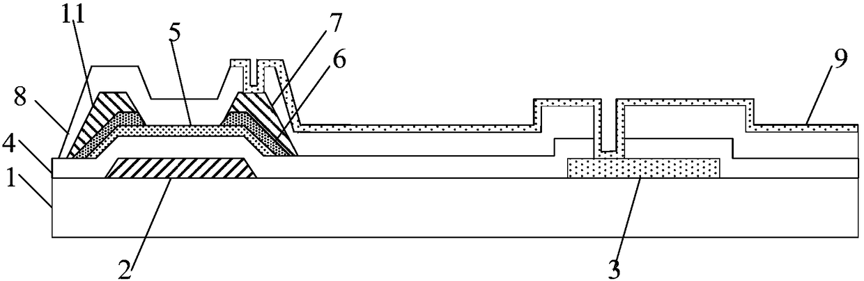
[0046] In this embodiment, before forming the first conductive pattern, a spacer pattern is formed at the bottom of the first conductive pattern. The spacer pattern can heighten the height of the first conductive pattern, thereby reducing...

Embodiment 2

[0052] This embodiment provides an array substrate. The array substrate includes a first conductive pattern on a base substrate, an insulating layer on the first conductive pattern, and a second conductive pattern on the insulating layer, The first conductive pattern and the second conductive pattern are connected by a via hole penetrating the insulating layer, wherein the array substrate further includes:

[0053] The spacer pattern located under the first conductive pattern, the orthographic projection of the spacer pattern on the base substrate and the orthographic projection of the via hole on the base substrate at least partially overlap.

[0054] In this embodiment, a spacer pattern is provided at the bottom of the first conductive pattern, and the spacer pattern can heighten the height of the first conductive pattern, thereby reducing the depth of the via hole at the first conductive pattern, and then on the array substrate When the alignment film is coated, the diffusion ef...

Embodiment 3

[0069] This embodiment provides a display device including the above-mentioned array substrate. The display device may be any product or component with a display function, such as an LCD TV, a liquid crystal display, a digital photo frame, a mobile phone, a tablet computer, etc., wherein the display device also includes a flexible circuit board, a printed circuit board, and a backplane.


PUM


Abstract

The invention provides an array substrate and a manufacture method thereof and a display device, and belongs to the technical field of display. The manufacture method comprises the following steps: forming an isolation pad pattern at a preset position on a substrate base plate; forming a first conductive pattern on the isolation pad pattern; forming an insulating layer comprising a via hole on the substrate base plate, where the first conductive pattern is formed; and forming a second conductive pattern on the insulating layer, wherein the first conductive pattern is connected with the second conductive pattern through the via hole running through the insulating layer; orthographic projection of the via hole on the substrate base plate and orthographic projection of the isolation pad pattern on the substrate base plate are at least partially overlapped. The technical scheme can prevent the defect of Mura, and improves display effect of the display device.

Description

Technical field [0001] The present invention relates to the field of display technology, in particular to an array substrate, a manufacturing method thereof, and a display device. Background technique [0002] In the prior art, the pixel electrode on the array substrate and the drain electrode of the thin film transistor are located in different layers, the pixel electrode and the drain electrode of the thin film transistor are covered with a passivation layer, and a conductive connection line is formed on the passivation layer. The pixel electrode and the drain electrode of the thin-film transistor are connected through the via hole penetrating the passivation layer. Because the thickness of the passivation layer is relatively large, the depth of the via hole is also relatively large, and the deep hole is prone to dents, resulting in an array substrate When the alignment film is coated, the alignment film is prone to spread unevenly at the deep holes, resulting in the problem of...

Claims


Application Information

Patent Timeline
Patent Type & Authority Patents(China)
IPC IPC(8): H01L27/12H01L21/77
CPCH01L27/124H01L27/1296
Inventor 程翔宇周波
Owner BOE TECH GRP CO LTD