

Light-emitting element reception package, light-emitting device and lighting device
A technology of light-emitting elements and light-emitting devices, which is applied in the direction of electrical components, semiconductor devices, and electric solid-state devices, and can solve problems such as unavailable, light-emitting wavelength deviation, and reduced efficiency, so as to suppress the reduction of luminous efficiency and improve light output or brightness. , The effect of improving the wavelength conversion efficiency
- Summary
- Abstract
- Description
- Claims
- Application Information
AI Technical Summary
Problems solved by technology
Method used
Image

Examples
Embodiment 1
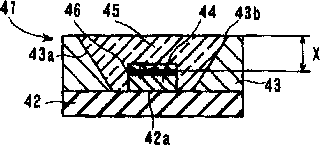
[0274] Examples of the light emitting device 41 according to the first embodiment of the present invention will be shown below.
[0275] First, an alumina ceramic matrix composed of crystal grains of various grain sizes to be the matrix 42 is prepared. Also, wiring conductors for electrically connecting the light emitting element 44 and an external circuit board via internal wiring formed inside the base body 42 are formed around the placement portion 42a where the light emitting element 44 is placed. Moreover, the metallization layer of the wiring conductor on the substrate 42 made of Mo-Mn powder is shaped into a circular pad with a diameter of 0.1 mm, and its surface is sequentially coated with a Ni plating layer with a thickness of 3 μm and an Au plating layer with a thickness of 2 μm. In addition, the internal wiring inside the base body 42 is formed by an electrical connection portion constituted by a through-conductor, a so-called through-hole. The via holes are also m...
Embodiment 2
[0282] Next, a light-emitting device 41 having the same structure as that of the above-mentioned example and in which the average grain size of the ceramic crystal grains after sintering of the substrate 42 is 1 (μm), 5 (μm), and 10 (μm) was produced, and the relative light emission to the direction was measured. The full beam (light output) of the load current of the element 44. Furthermore, the light-emitting device 41 was installed in heat radiation equipment with the same cooling function everywhere, and the light output was measured with an integrating sphere. The result is as Figure 7 shown.
[0283] Such as Figure 27 As shown, when the rated current of the load current to the light-emitting element 44 is 20 (mA) and the rated voltage is 3.4 (V), the light emission of the light-emitting device 41 with the average grain size of ceramic crystal grains being 1 (μm) The output was 0.96 (lm), and the luminous efficiency was 14 (lm / W). In addition, the light output of th...
Embodiment 3
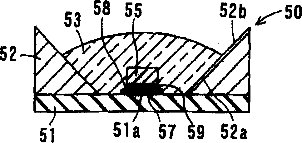
[0288] according to Figure 7 , for the light emitting device 60C of the sixth embodiment of the present invention, examples are shown below.
[0289] First, an alumina ceramic substrate to be the base body 61 is prepared. Furthermore, the base 61 is integrally formed with the convex portion 61b having the seating portion 61a, and the upper surface of the seating portion 61a is parallel to the upper surface of the base 61 at a location other than the seating portion 61a.
[0290] The base body 61 has a cylindrical convex portion 61b having a diameter of 0.4mm×thickness (various values) formed on the upper central portion of a cylindrical plate having a diameter of 0.8mm×thickness 0.5mm.
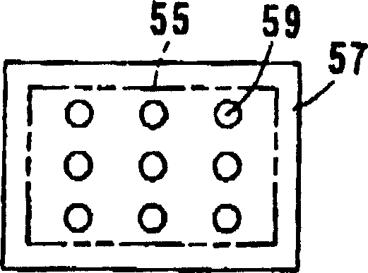
[0291] In addition, an electrical connection pattern for electrically connecting the light emitting element 65 and an external circuit board through internal wiring formed inside the base body 61 is formed on the mounting portion 61a of the convex portion 61b where the light emitting element...
PUM
 Abstract
Description
Claims
Application Information