Electronic component test sorting equipment

A technology of electronic components and sorting equipment, which is applied in the field of electronic component testing and sorting equipment, can solve problems such as complex mechanism, complicated mechanism and transportation path, and increased complexity of transportation path

Active Publication Date: 2019-02-22
HON PRECISION INC
View PDF10 Cites 0 Cited by
  • Summary
  • Abstract
  • Description
  • Claims
  • Application Information

AI Technical Summary

Problems solved by technology

[0004] 1. The mechanism and conveying path are relatively complicated: the input device 14 must be provided with a first feeding carrier 145, a second feeding carrier 146, a first discharging carrier 147 and a second feeding carrier capable of moving in the X axis. The discharge carrier 148, therefore not only the mechanism is more complicated, but also must pass through the first material feed carrier 145, the second material feed carrier 146, the first discharge carrier 147 and the second discharge carrier 148 for X-axis Mobile transfer increases the complexity of the conveying path and affects the cost of the equipment
[0005] 2. The number of times and time for exchanging and transferring are relatively large: the feeding and transferring arm 141 of the input device 14 must pass through the transfer of the first feeding carrier 145 and the second feeding carrier 146, so that the electrons to be tested can be transferred. Components are transferred to the first pressing arm 143 or the second pressing arm 144 and moved into the testing device 13, and the first pressing arm 143 and the second pressing arm 144 must pass through the first discharge carrier 147 or the second discharge carrier. The transfer of the platform 148 can transfer the completed electronic components to the discharge transfer arm 142 and transfer to the receiving device 12. Therefore, not only the number of times of exchange and transfer is large, but also the time for exchange and transfer is too long, which affects the Test capacity

Method used


Image

  • Electronic component test sorting equipment
  • Electronic component test sorting equipment
  • Electronic component test sorting equipment

Examples


Embodiment Construction

[0052] In order to make your review committee members have a further understanding of the present invention, the preferred embodiments are hereby given in conjunction with the drawings, and are described in detail as follows:

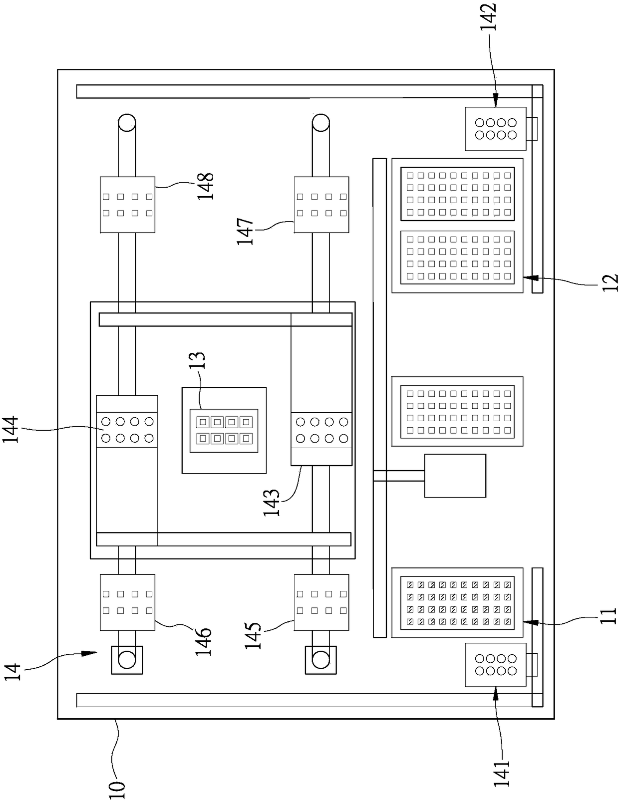
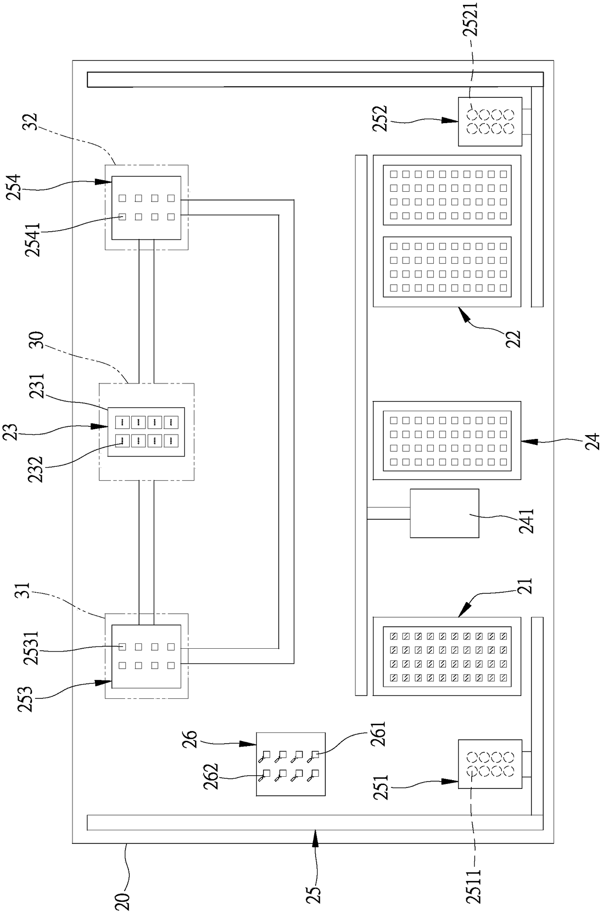
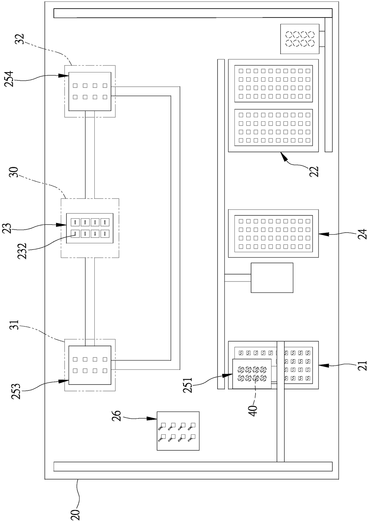
[0053] see figure 2 , the testing and sorting equipment of the first embodiment of the present invention, it is equipped with feeding device 21, material receiving device 22, testing device 23, empty plate device 24, conveying device 25 and alignment device 26 on machine platform 20, in addition In terms of area space, the machine 20 is provided with a test area 30, a first exchange area 31 located at the first side of the test area 30, and a second exchange area 32 located at the second side of the test area 30. The feeding device 21 Accommodate a plurality of electronic components to be tested with electrical contacts facing upwards, the receiving device 22 accommodates a plurality of tested electronic components of different grades, and the testing ...


PUM


Abstract

The invention provides a testing and sorting device for electronic elements. The testing and sorting device comprises a feeding device, a collecting device, a testing device and a conveying device, wherein the feeding device accommodates a plurality of to-be-tested electronic elements of which electric contacts are upward; the collecting device accommodates a plurality of tested electronic elements of different grades; the testing device is arranged above a testing zone, and performs testing operation on the electronic elements of which the electric contacts are upward; the conveying device is provided with at least one feeding transfer arm, at least one discharge transfer arm and at least one testing transfer arm; the feeding transfer arm transfers the electronic elements of which the electric contacts are upward at the feeding device from the upper side to the testing transfer arm located in a first exchange zone; the testing transfer arm bears the electronic elements from the lower side, transfers the electronic elements to the testing zone, electrically connects the electronic elements and the testing device with the electric contacts being upward, performs testing operation, and transfers the electronic elements to a second exchange zone after testing; and the discharge transfer arm transfers the electronic elements to the collecting device from the upper side, and performs sorting operation.

Description

technical field [0001] The invention relates to an electronic component testing and sorting equipment that utilizes an upward transfer and testing method of the electrical contacts of the electronic component to effectively simplify the conveying path, effectively reduce the equipment cost and improve the testing capacity. Background technique [0002] By the way, under the continuous research and development and innovation of today's technology, the work that must be completed by the combination of many large electronic circuits in the past has been completely replaced by integrated circuits (IC for short), because ICs are processed in multiple channels during the production process. Therefore, in order to ensure product quality, after the IC is produced, the industry will conduct circuit testing operations to detect whether the IC is damaged during the production process, and then detect defective products. [0003] see figure 1 , which is the Chinese Taiwan Invention No....

Claims


Application Information

Patent Timeline
Patent Type & Authority Patents(China)
IPC IPC(8): B07C5/344B07C5/36G01R31/00
Inventor 谢旼达张原龙
Owner HON PRECISION INC
Why Eureka
Try Eureka