

Semiconductor device and design device
A technology of semiconductors and computing processing devices, which is applied in the direction of measuring devices, CAD circuit design, computer-aided design, etc., and can solve problems affecting test costs and other issues
- Summary
- Abstract
- Description
- Claims
- Application Information
AI Technical Summary
Problems solved by technology
Method used
Image

Examples
no. 1 example
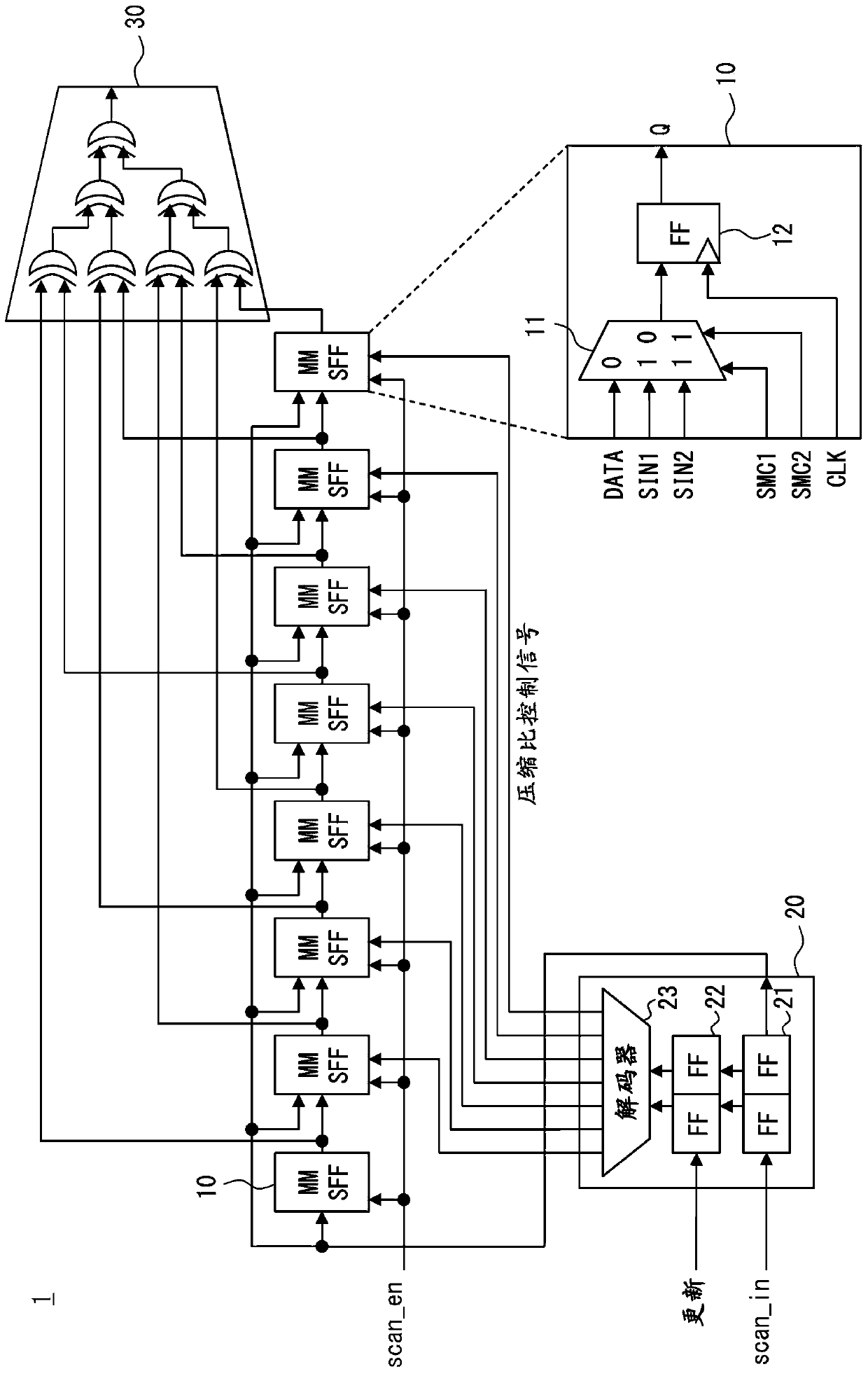
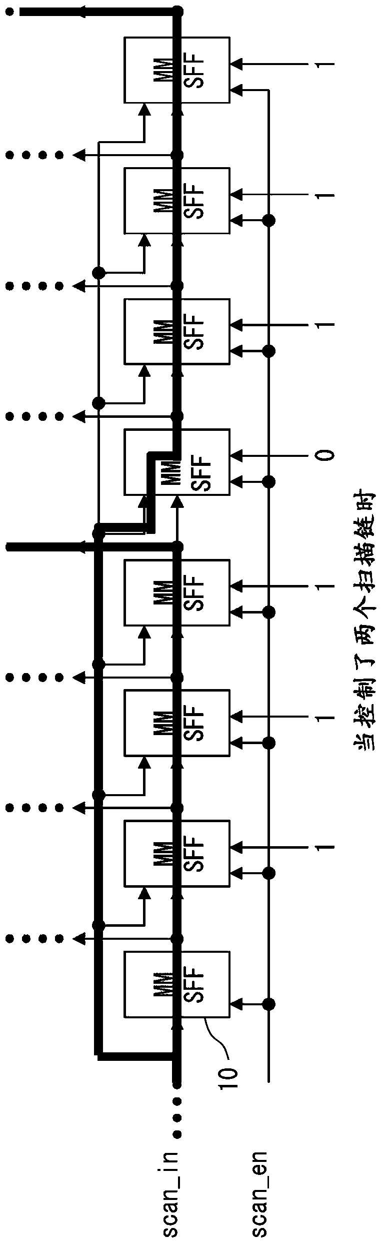
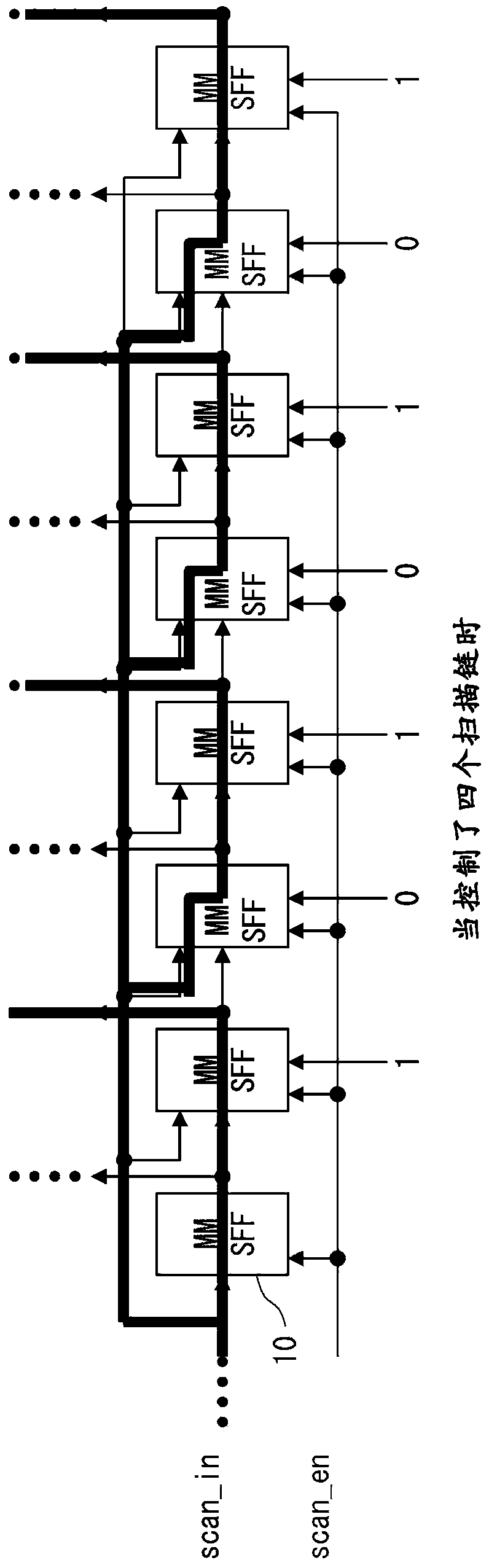
[0040] The following should refer to figure 1 A semiconductor device according to the first embodiment is explained. figure 1 is a schematic diagram showing the configuration of the semiconductor device 1 according to the first embodiment. Such as figure 1As shown, a semiconductor device 1 includes a plurality of MMSFFs (Multimode Support Scan Flip Flops) 10 , a multimode control circuit 20 , and a compressor 30 . In this example, scan chain configurations with different numbers of scan chains shall be called modes individually, and multiple modes shall be called multi-mode. The multi-mode support scan flip-flop is a flip-flop that can have multiple scan chain configurations, and the multiple scan chain configurations have different compression ratios by selecting and outputting external input test signals or shift test signals.
[0041] In the semiconductor device 1, one or more MMSFFs 10 are connected in series to thereby establish one or more scan chains. The expande...
no. 2 example
[0073] The following should refer to Figure 5 A semiconductor device according to the second embodiment is explained. Figure 5 is a schematic diagram showing the configuration of a semiconductor device 1A according to the second embodiment. Such as Figure 5 As shown, a semiconductor device 1A includes a plurality of MMSFFs 10, a multimode control circuit 20, and a variable compression ratio compressor 30A. The difference between the first embodiment and the second embodiment is that in the second embodiment, instead of the compressor 30 included in the first embodiment, a variable compressor 30A is included.
[0074] The variable compressor 30A can change the compression ratio according to the number of scan chains. The variable compressor 30A includes an XOR (exclusive OR) tree and a MUX (multiplexer) 31 (31a to 31c). The output from each MMSFF 10 is input to the XOR gates that make up the XOR tree. For example, if Figure 5 As shown, the output from the first and fi...
no. 3 example
[0080] The following should refer to Figure 6 A semiconductor device according to the third embodiment is explained. Figure 6 is a schematic diagram showing the configuration of the semiconductor device 1B according to the third embodiment. Such as Figure 6 As shown, the semiconductor device 1B includes a plurality of MMSFFs 10 , a multimode control circuit 20 , a variable compression ratio compressor 30B, and a mask control circuit 40 . The second embodiment differs from the third embodiment in that in the third embodiment, a variable compressor 30B is included instead of the variable compressor 30A included in the second embodiment, and a variable compressor 30B for controlling Masking control circuit 40 of transcompressor 30B.
[0081] In a similar manner to variable compressor 30A, variable compressor 30B includes MUX 31 (31a to 31c). Further, in the first stage, masking circuits 32 are respectively provided to the input sides of the four XOR gates. More specifical...
PUM
 Abstract
Description
Claims
Application Information