Ultrathin atomic layer deposition film accuracy thickness control

A technology of atomic layer deposition and deposition temperature, which is applied in coating, metal material coating process, semiconductor/solid-state device manufacturing, etc., can solve the problems that are not suitable for ultra-thin films

Active Publication Date: 2016-10-05
LAM RES CORP
View PDF9 Cites 9 Cited by
  • Summary
  • Abstract
  • Description
  • Claims
  • Application Information

AI Technical Summary

Problems solved by technology

However, existing ALD processes may not be suitable for depositing ultra-thin films with thicknesses below about 50 angstroms
For example, many existing ALD processes for depositing ultra-thin films result in large wafer-to-wafer variations between films deposited from substrate to substrate

Method used


Image

  • Ultrathin atomic layer deposition film accuracy thickness control
  • Ultrathin atomic layer deposition film accuracy thickness control
  • Ultrathin atomic layer deposition film accuracy thickness control

Examples


Embodiment Construction

[0089] In the following description, numerous specific details are set forth in order to provide a thorough understanding of the presented embodiments. The disclosed embodiments may be practiced without some or all of these specific details. In other instances, well known process operations have not been described in detail to avoid unnecessarily obscuring the disclosed embodiments. While the disclosed embodiments will be described in conjunction with specific embodiments, it will be understood that no limitation to the disclosed embodiments is intended.

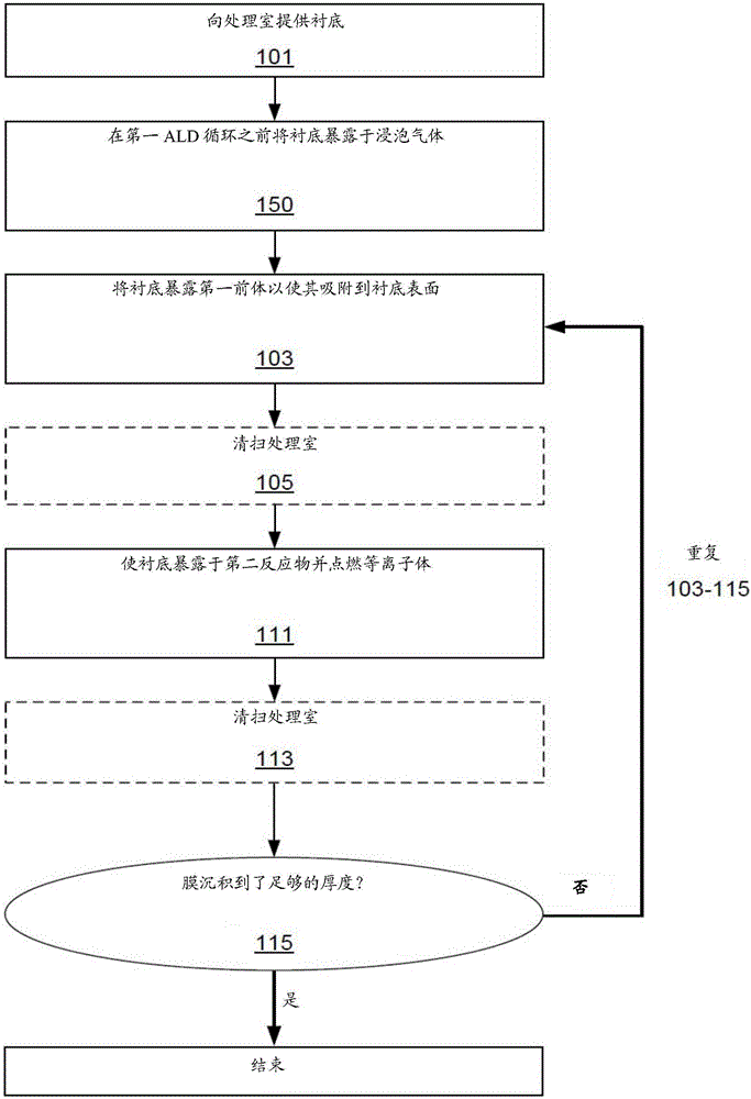
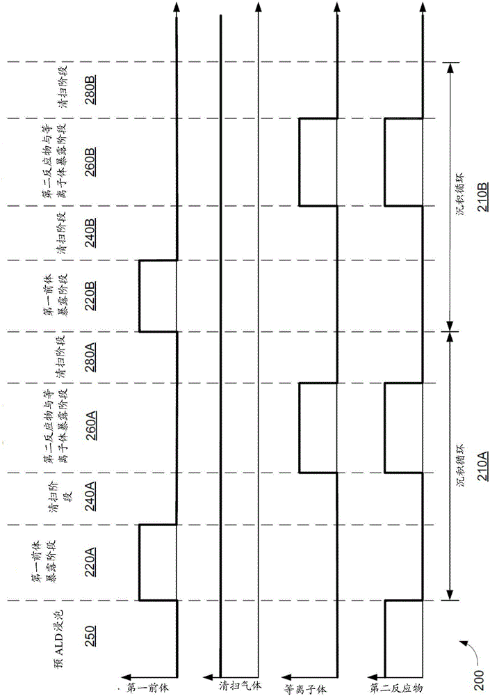
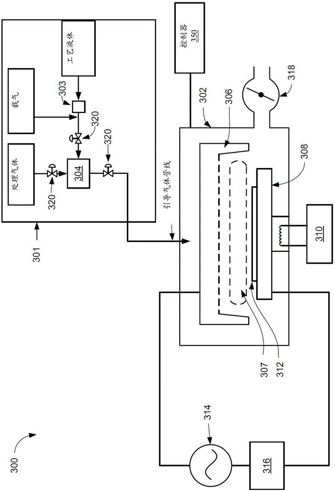
[0090] Fabrication of semiconductor devices typically involves depositing one or more conformal thin films on a substrate in an integrated fabrication process. For example, some front-end-of-the-line processes involve the deposition of conformal films by atomic layer deposition (ALD). ALD is a technique for depositing thin layers of materials using a continuous self-limiting reaction. The ALD process uses a surface-mediated...


PUM

PropertyMeasurementUnit
thicknessaaaaaaaaaa
thicknessaaaaaaaaaa
diameteraaaaaaaaaa

Abstract

The present invention relates to ultrathin atomic layer deposition film accuracy thickness control. Methods for depositing ultrathin films by atomic layer deposition with reduced wafer-to-wafer variation are provided. Methods involve exposing the substrate to soak gases including one or more gases used during a plasma exposure operation of an atomic layer deposition cycle prior to the first atomic layer deposition cycle to heat the substrate to the deposition temperature.

Description

technical field [0001] The invention generally relates to the field of semiconductor processing, in particular to the precise control of the thickness of an ultra-thin atomic layer deposition film. Background technique [0002] Various thin film layers for semiconductor devices can be deposited using atomic layer deposition (ALD) processes. However, existing ALD processes may not be suitable for depositing ultra-thin films with a thickness below about 50 Angstroms. For example, many existing ALD processes for depositing ultra-thin films result in large wafer-to-wafer variations between the films deposited on the substrate from substrate to substrate. Contents of the invention [0003] The present invention provides methods and apparatus for processing semiconductor substrates. One aspect relates to a method for depositing a silicon oxide film on a semiconductor substrate by atomic layer deposition, the method comprising: (a) inserting the substrate into a chamber; (b) in...

Claims


Application Information

Patent Timeline
Patent Type & Authority Applications(China)
IPC IPC(8): H01L21/205H01L21/316C23C16/40C23C16/44
CPCH01L21/205C23C16/401C23C16/45525H01L21/02126H01L21/02312H01L21/02521H01J37/32899C23C16/02C23C16/402C23C16/45534C23C16/45551C23C16/45553C23C16/52H01L21/0228H01L21/02164H01L21/02211H01L21/02274C23C16/45542H01J37/32449H01J37/32743H01J37/32834H01J2237/1825H01J2237/201H01J2237/20278H01J2237/332
Inventor 钱俊康胡阿德里安·拉沃伊松山清治普鲁肖塔姆·库马尔
Owner LAM RES CORP
Why Eureka
Try Eureka