
Wafer Thinning Methods

A wafer and ring-shaped technology, applied in the manufacturing of electrical components, circuits, semiconductor/solid-state devices, etc., can solve the problems of low production efficiency, easy warpage deformation, fragile wafers, etc., to achieve a wide range of tolerance, The effect of ensuring efficiency, reducing process difficulty and complexity

Active Publication Date: 2019-05-28
SEMICON MFG INT (SHANGHAI) CORP
View PDF6 Cites 0 Cited by
  • Summary
  • Abstract
  • Description
  • Claims
  • Application Information

AI Technical Summary

Problems solved by technology

[0004] However, when the wafer is thinned below a certain thickness, the wafer becomes extremely brittle, such as warping, deforming or even chipping
However, in order to avoid wafer cracking and deformation as far as possible in the existing technology, many restrictions are imposed on various processes during wafer production and bonding, which will lead to lower overall production efficiency.

Method used


Image

  • Wafer Thinning Methods
  • Wafer Thinning Methods
  • Wafer Thinning Methods

Examples


Embodiment Construction

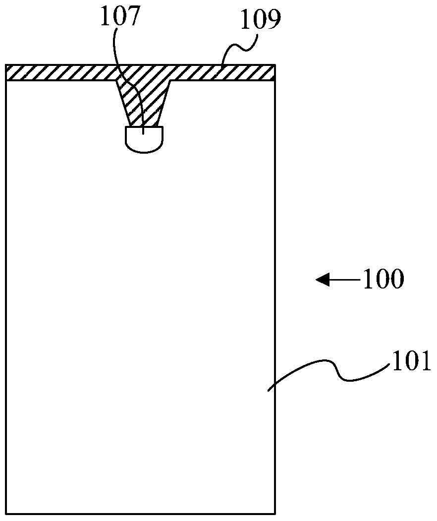
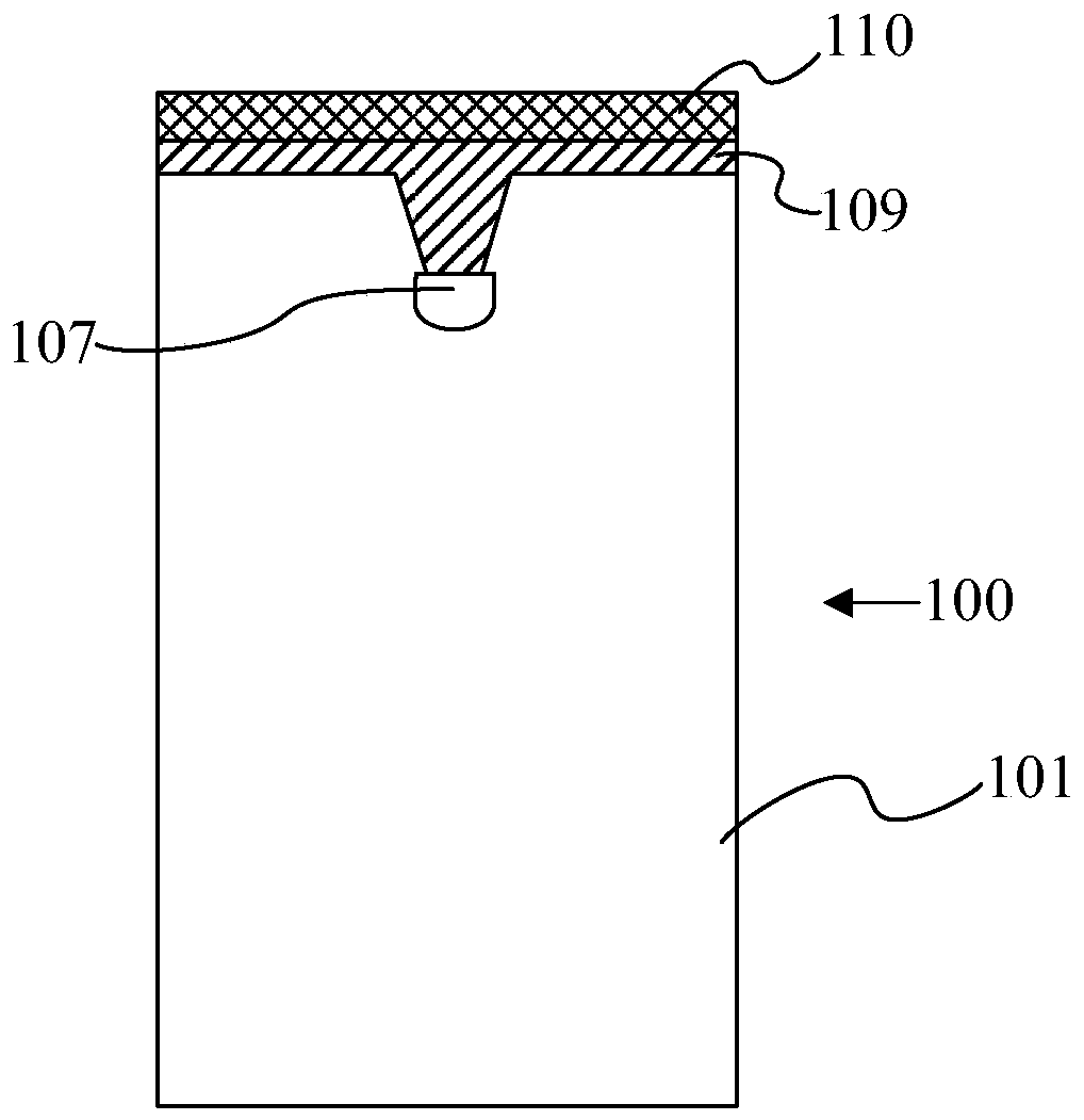
[0045] In order to reduce cracks or warping of the wafer when the wafer is thinned, in the prior art, the wafer to be thinned is adhered to a pad wafer by glue in advance before the wafer is thinned, and then A thinning process is performed on the tape thinned wafer attached to the pad wafer. The thinned wafer is then removed from the backing wafer for use. However, this method has a small range of temperature tolerance, especially high temperature, because the glue may start to decompose or soften at a slightly higher temperature (higher than 100 degrees Celsius), which will lead to thinned wafers and The gasket wafers cannot be tightly fixed, which may cause cracks or warping of the wafer to be thinned during the thinning process.

[0046] At the same time, in order not to make the temperature too high in the prior art, the ambient temperature of the wafer has to be kept within a certain temperature. But this will affect the progress of other processes, bring troubles to t...


PUM


Abstract

The present invention provides a wafer thinning method. The method comprises: providing a first wafer to be thinned, wherein the first wafer includes a right side configured to form a semiconductor device and a back side relative to the right side; forming a first inorganic material layer at the right side of the first wafer; providing a second wafer configured to support the first wafer, wherein the second wafer includes a work surface configured to match the right side of the first wafer; forming a second inorganic material layer on the work surface of the second wafer; bonding the first inorganic material layer and the second inorganic material layer to bond the first wafer and the second wafer; removing the partial materials of the back side of the first wafer to perform thickness thinning process of the first wafer; and bonding the thinned first wafer and the second wafer. The bearing capacity for the environment temperature is widened so as to facilitate reducing the difficulty and the complexity of other technologies and ensure the efficiency of the whole technology.

Description

technical field [0001] The invention relates to the field of semiconductor manufacturing, in particular to a wafer thinning method. Background technique [0002] Packaging technology is essentially a chip packaging technology. This packaging is necessary for the chip because the chip must be isolated from the outside world to prevent impurities in the air from corroding the chip circuit and causing electrical performance degradation. On the other hand, packaged chips are also easier to install and transport. The quality of the packaging technology directly affects the performance of the chip itself and the design and manufacture of the printed circuit board connected to it. [0003] The current packaging technology has gradually transitioned from surface mount technology and ball grid array terminal packaging technology (Ball GridArray, BGA) to three-dimensional packaging technology (3D Package). Three-dimensional packaging technology can be divided into three-dimensional ...

Claims


Application Information

Patent Timeline
Patent Type & Authority Patents(China)
IPC IPC(8): H01L21/304
Inventor 施林波陈福成刘尧
Owner SEMICON MFG INT (SHANGHAI) CORP
Learn More