Chip packaging structure and manufacture method thereof

A technology of chip packaging structure and manufacturing method, which is applied in the fields of printed circuit manufacturing, semiconductor/solid-state device manufacturing, circuit heating device, etc., can solve problems such as occupied volume and design restrictions, and achieve improved reliability, reduced stress, and improved heat dissipation effect of effect

Inactive Publication Date: 2016-10-05
ALI CORP
View PDF6 Cites 3 Cited by
  • Summary
  • Abstract
  • Description
  • Claims
  • Application Information

AI Technical Summary

Problems solved by technology

However, the external heat sink will take up a lot of volume, thus creating design constraints for the overall electronics enclosure

Method used


Image

  • Chip packaging structure and manufacture method thereof
  • Chip packaging structure and manufacture method thereof
  • Chip packaging structure and manufacture method thereof

Examples


Embodiment Construction

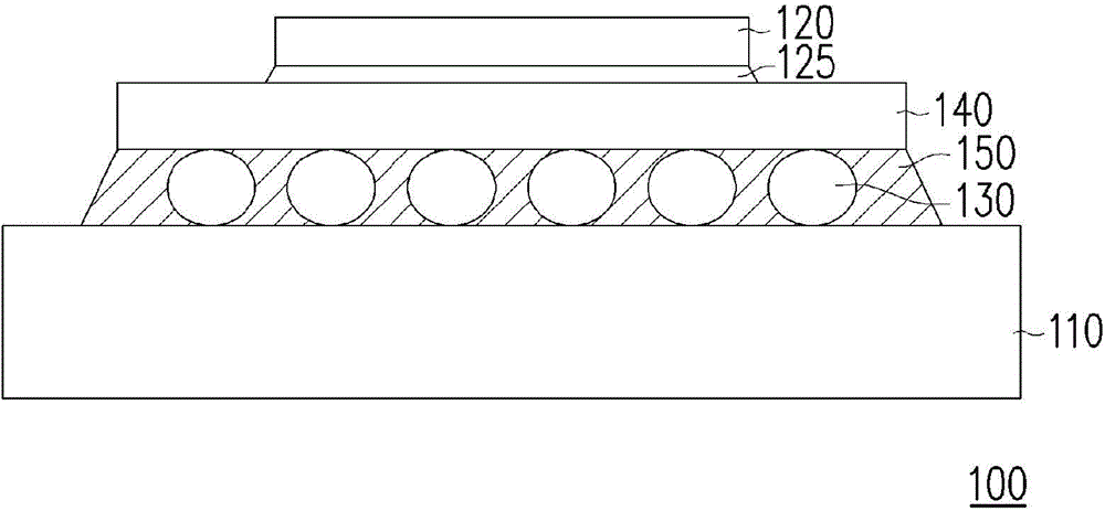
[0047] figure 1 is a schematic diagram of a chip package structure according to an embodiment of the present invention. Please refer to figure 1The chip packaging structure 100 includes a substrate 110 , at least one chip 120 , a plurality of conductive bumps 130 and an insulating and thermally conductive material 150 . In this embodiment, the chip 120 is disposed on the chip carrier 140 , and the chip carrier 140 is disposed on the substrate 110 . In addition, the conductive bump 130 is disposed between the substrate 110 and the chip carrier 140 to electrically connect the substrate 110 and the chip 120 . Furthermore, the insulating and thermally conductive material 150 is disposed between the conductive bumps 130 and covers the conductive bumps 130 . In this embodiment, the substrate 110 is, for example, a printed circuit board (PCB) or a flexible circuit board (flexible circuit board). The conductive bumps 130 are, for example, solder bumps, copper pillars, copper stud ...


PUM


Abstract

The invention provides a chip packaging structure and a manufacture method thereof. The chip packaging structure includes a substrate, at least one chip, a plurality of conductive bumps, and an insulating thermally conductive material. The chip is disposed on a chip carrier, and the chip carrier is disposed on the substrate. The conductive bumps are disposed between the substrate and the chip carrier to electrically connect the substrate with the chip. The insulating thermally-conductive material is disposed between the conductive bumps and covers the conductive bumps.

Description

technical field [0001] The invention relates to a chip packaging technology, and in particular to a chip packaging structure with insulating and heat-conducting materials and a manufacturing method thereof. Background technique [0002] In the semiconductor industry, the production of integrated circuits (Integrated Circuits, IC) is mainly divided into three stages: wafer (Wafer) manufacturing, integrated circuit fabrication, and integrated circuit packaging (Package). Chips are completed through steps such as wafer fabrication, circuit design, photomask fabrication, and wafer dicing. Each chip formed by dicing the wafer can be covered with a sealing material after being electrically connected to external signals through the contacts on the chip. The purpose of its packaging is to prevent the chip from being affected by moisture, heat, and noise, and to provide a medium for electrical connection between the chip and the external circuit, thus completing the packaging step o...

Claims


Application Information

Patent Timeline
Patent Type & Authority Applications(China)
IPC IPC(8): H01L23/498H01L23/373H01L21/48
CPCH01L23/562H01L23/49816H01L24/16H01L24/32H01L24/48H01L24/81H01L24/83H01L2223/54426H01L2224/16227H01L2224/32225H01L2224/48227H01L2224/73204H01L2224/83862H01L2924/15311H01L23/544H01L2223/54486H05K1/0206H05K1/0209H05K3/3436H05K2201/10977H01L2924/00014H01L2924/351H01L2924/3512H01L2224/45099H01L2224/16225H01L2924/00H01L23/367
Inventor 张育儒高志宏陈芝莹
Owner ALI CORP
Why Eureka
Try Eureka