Polarization-insensitive micro-ring filter based on silicon nanowire waveguide

A polarization-insensitive, silicon nanowire technology, used in light guides, instruments, optics, etc., can solve problems such as increasing device size and increasing system complexity, reducing complexity and improving flexibility.

Active Publication Date: 2016-10-26
ZHEJIANG UNIV
View PDF9 Cites 14 Cited by
  • Summary
  • Abstract
  • Description
  • Claims
  • Application Information

AI Technical Summary

Problems solved by technology

To a certain extent, the complexity of the system is increased,...

Method used


Image

  • Polarization-insensitive micro-ring filter based on silicon nanowire waveguide
  • Polarization-insensitive micro-ring filter based on silicon nanowire waveguide
  • Polarization-insensitive micro-ring filter based on silicon nanowire waveguide

Examples


Embodiment 1

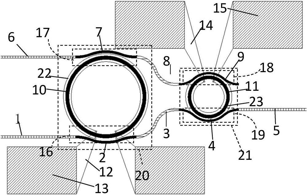
[0037] Such as figure 1 As shown, the first embodiment includes a connected first microring filter 20 and a second microring filter 21 and metal electrodes, the first microring filter 20 includes a first ring waveguide 10 and a symmetrically placed ring waveguide The first curved waveguide 2 and the third curved waveguide 7 on both sides of 10, the microring adopts a single first ring waveguide 10, and the second microring filter 21 includes the second ring waveguide 11 and the second The second curved waveguide 4 and the fourth curved waveguide 9 on both sides of the ring waveguide 11, wherein the micro-ring adopts a single second ring waveguide 11. The first ring waveguide 10 and the second ring waveguide 11 adopt a single microring structure.

[0038] The input waveguide 1, the first curved waveguide 2, the first adiabatic connection waveguide 3, the second curved waveguide 4 and the first output waveguide 5 are connected end to end, and are located on the same side of the...

Embodiment 2

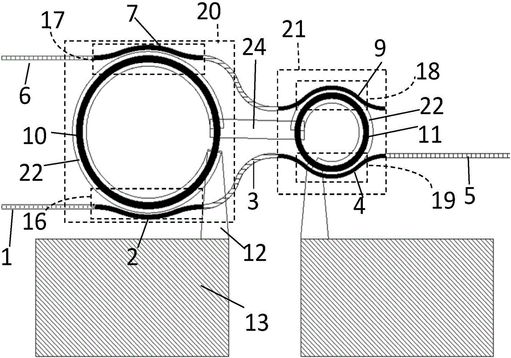
[0045] Such as figure 2 As shown, the second embodiment includes a connected first microring filter 20 and a second microring filter 21 and metal electrodes. The first microring filter 20 includes a first ring waveguide 10 and a symmetrically placed ring waveguide The first curved waveguide 2 and the third curved waveguide 7 on both sides of 10, the microring adopts a single first ring waveguide 10, and the second microring filter 21 includes the second ring waveguide 11 and the second The second curved waveguide 4 and the fourth curved waveguide 9 on both sides of the ring waveguide 11, wherein the micro-ring adopts a single second ring waveguide 11. The first ring waveguide 10 and the second ring waveguide 11 adopt a single microring structure.

[0046] The input waveguide 1, the first curved waveguide 2, the first adiabatic connection waveguide 3, the second curved waveguide 4 and the first output waveguide 5 are connected end to end, and are located on the same side of t...

Embodiment 3

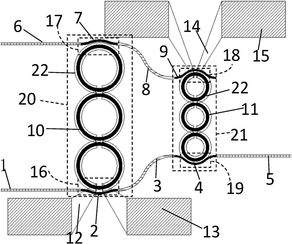
[0049] Such as figure 1 As shown, the third embodiment includes a first micro-ring filter 20, a second micro-ring filter 21 and metal electrodes connected to each other. The first micro-ring filter 20 includes three cascaded first ring waveguides 10 and symmetrically arranged The first curved waveguide 2 and the third curved waveguide 7 on both sides after cascading the first ring waveguide 10, the second microring filter 21 includes three cascaded second ring waveguides 11 and the second ring waveguide symmetrically placed 11 After cascading, the second curved waveguide 4 and the fourth curved waveguide 9 on both sides. The first ring waveguide 10 and the second ring waveguide 11 adopt a cascaded structure of multiple microrings.

[0050] The input waveguide 1, the first curved waveguide 2, the first adiabatic connection waveguide 3, the second curved waveguide 4 and the first output waveguide 5 are connected end to end, and are located on the same side after the first ring ...


PUM


Abstract

The invention discloses a polarization-insensitive micro-ring filter based on a silicon nanowire waveguide. The polarization-insensitive micro-ring filter comprises a first micro-ring filter and a second micro-ring filter, wherein a heating electrode used for adjusting resonant wavelength is arranged above each of the first micro-ring filter and the second micro-ring filter, the first micro-ring filter and the second micro-ring filter operate in a single-polarization and have the same resonant wavelength, the first micro-ring filter and the second micro-ring filter are respectively used for filtering in a TM polarization mode and a TE polarization mode in an interchangeable manner, each micro-ring filter is provided with a group of metal regions or the micro-ring filters are provided with the same group of metal regions, and the resonant wavelength is corrected through heating the two groups of metal electrodes or combining with a laser oxidizing waveguide. The polarization-insensitive micro-ring filter disclosed by the invention has the advantages of small size and simple structure, and provides a feasible scheme for solving the polarization sensitive problem of the micro-loop filter.

Description

technical field [0001] The invention belongs to the field of integrated optoelectronic devices, in particular to a polarization-insensitive microring filter based on a silicon nanowire waveguide. Background technique [0002] Microring filters are favored in the field of integrated optical devices because of their small size, simple structure, and flexible functional characteristics. The silicon nanowire waveguide based on the silicon on insulator (Silicon On Insulator, SOI) material platform has an ultra-high refractive index difference and a strong ability to confine the optical field, so it can realize an ultra-compact integrated optical device structure, and has a CMOS process compatible characteristic. This series of advantages makes microring filters based on silicon nanowire waveguides one of the hotspots of researchers. [0003] Silicon nanowire waveguide has strong birefringence characteristics, that is, the effective refractive index of light with different polar...

Claims


Application Information

Patent Timeline
IPC IPC(8): G02B6/293
CPCG02B6/2934G02B6/29397
Inventor 戴道锌谭莹
Owner ZHEJIANG UNIV
Why Eureka
Try Eureka