

Constructing method of noise model for millimeter waves FET
A technology of noise model and establishment method, applied in special data processing applications, instruments, electrical digital data processing, etc., can solve the problem of poor accuracy of FET noise model, achieve the effect of high model accuracy and avoid parasitic parameter extraction
- Summary
- Abstract
- Description
- Claims
- Application Information
AI Technical Summary
Problems solved by technology
Method used
Image


Examples
Embodiment Construction
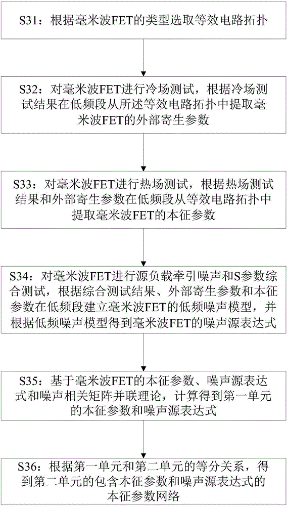
[0024] The following will clearly and completely describe the technical solutions in the embodiments of the present invention with reference to the accompanying drawings in the embodiments of the present invention. Obviously, the described embodiments are only some, not all, embodiments of the present invention. Based on the embodiments of the present invention, all other embodiments obtained by persons of ordinary skill in the art without making creative efforts belong to the protection scope of the present invention.
[0025] see figure 1 , is a schematic flowchart of a method for establishing a noise model of a millimeter-wave FET according to an embodiment of the present invention. The noise model establishment method of the embodiment of the present invention comprises the following steps:
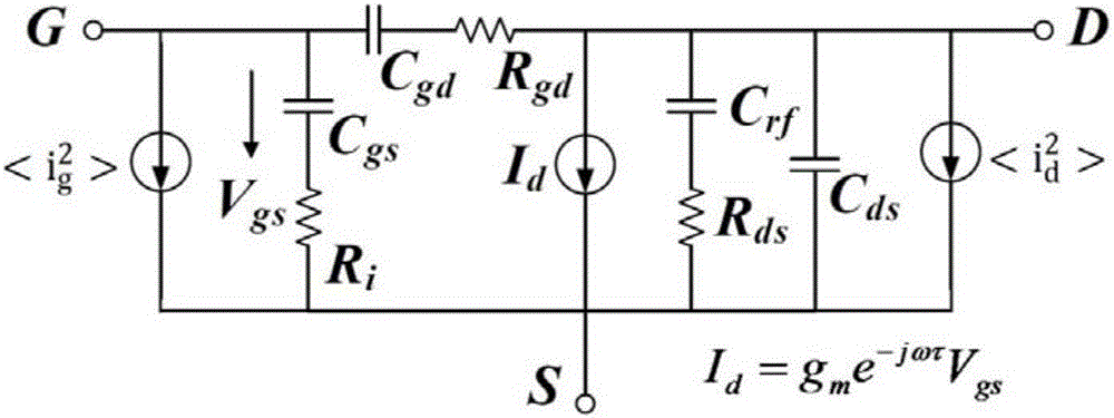
[0026] S1: Divide the millimeter-wave FET into a passive structure area and an active structure area, where the passive structure area includes input electrodes and output electrodes...
PUM
 Abstract
Description
Claims
Application Information