GaN HEMT equivalent circuit topological structure based on novel resistance model

A resistance model and equivalent circuit technology, applied in CAD circuit design, electrical digital data processing, special data processing applications, etc., can solve problems such as changes, and achieve the effect of great practical significance and high model accuracy

Pending Publication Date: 2021-02-19
TIANJIN UNIV
View PDF12 Cites 0 Cited by
  • Summary
  • Abstract
  • Description
  • Claims
  • Application Information

AI Technical Summary

Problems solved by technology

[0010] To sum up, in order to solve the existing parasitic resistance parameter R s For the problem of changing with the change of drain-source cu

Method used


Image

  • GaN HEMT equivalent circuit topological structure based on novel resistance model
  • GaN HEMT equivalent circuit topological structure based on novel resistance model
  • GaN HEMT equivalent circuit topological structure based on novel resistance model

Examples


Example Embodiment

[0040]In order to make the technical means realized by the present invention easier to understand, the application will be further described in detail below with reference to the accompanying drawings and embodiments.
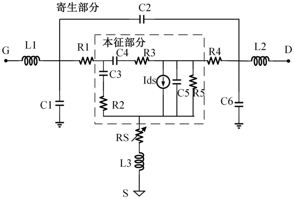
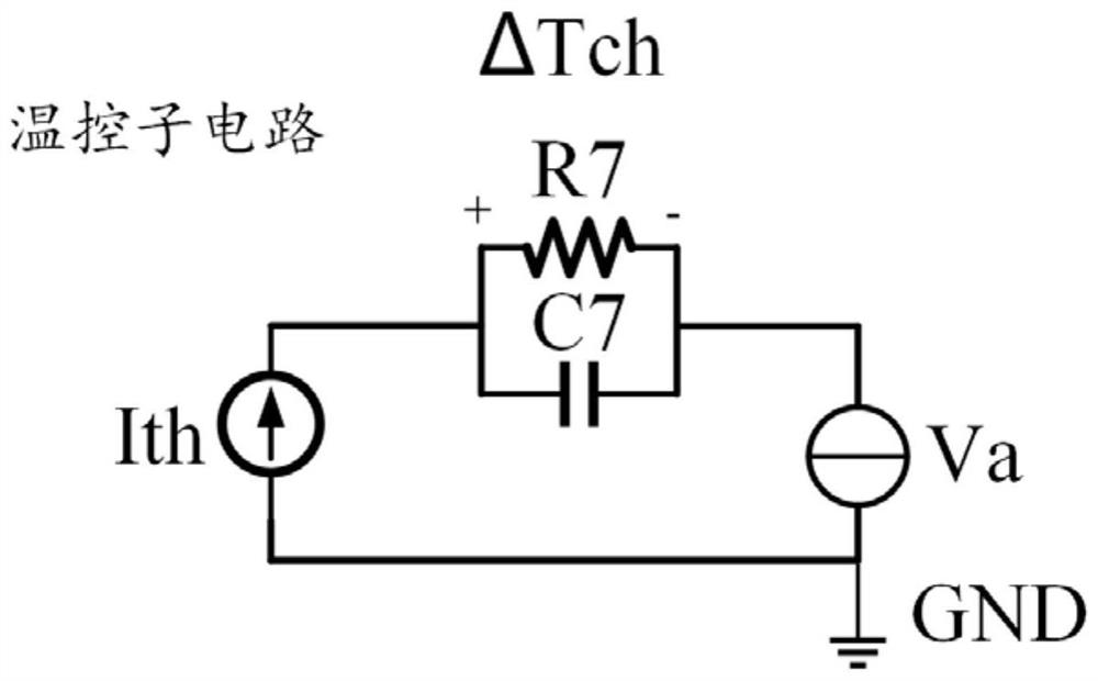
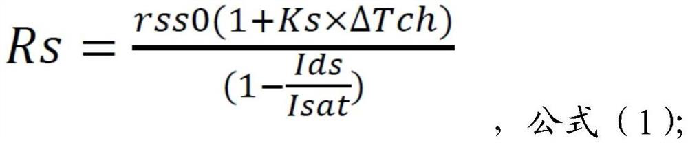
 It is understandable that the specific embodiments described here are only used to explain the related application, but not to limit the application. In addition, it should be noted that, for ease of description, only parts related to the present application are shown in the drawings.

[0041]It should be noted that the embodiments in the application and the features in the embodiments can be combined with each other if there is no conflict. Hereinafter, the present application will be described in detail with reference to the drawings and in conjunction with embodiments.

[0042]Seefigure 1 ,figure 2 The present invention provides a GaN HEMT equivalent circuit topology based on a new resistance model, which is an embedded nonlinear resistance parameter RsThe model GaN HEMT ...


PUM


Abstract

The invention discloses a GaN HEMT equivalent circuit topological structure based on a novel resistance model. The GaN HEMT equivalent circuit topological structure comprises a transistor GH, whereina grid G, a source S and a drain D of the GH are respectively connected with one ends of inductors L1, L3 and L2; the other end of the L1 is connected with one end of a capacitor C1, one end of a resistor R1 and one end of a capacitor C2; the other end of the resistor R1 is respectively connected with one end of a capacitor C3 and one end of a capacitor C4; the other end of the C3 is connected with one end of a resistor R2; the other end of the capacitor C4 is connected with one end of a resistor R3; the other end of the resistor R3 is respectively connected with one end of a current source Ids, a capacitor C5, a resistor R5 and one end of a resistor R4; and the other end of the resistor R2 is respectively connected with one end of the resistor RS, the other end of the current source Ids,the other end of the C5 and the other end of the R5. According to the GaN HEMT equivalent circuit topological structure, a novel parameter Rs model of the resistor RS is adopted, so a problem that theparameter Rs of the resistor RS changes along with the change of drain-source current and temperature can be solved.

Description

technical field [0001] The invention relates to the technical field of semiconductor device modeling, in particular to a GaN HEMT equivalent circuit topology based on a novel resistance model. Background technique [0002] With the expansion of the application field of semiconductor devices, semiconductors are required to be strong in high temperature, strong radiation and high power environments in special occasions, so silicon carbide (SiC), gallium nitride (GaN), zinc oxide (ZnO), diamond , aluminum nitride (AlN) as the representative of the third generation of semiconductor materials on the stage of history. [0003] Compared with the first and second generation semiconductor materials, the third-generation semiconductor materials represented by GaN materials have the following advantages: [0004] 1. The band gap of GaN material is very large (3.39eV), which makes it have good heat resistance and can work above 500 °C; [0005] 2. The GaN material has a high breakdown...

Claims


Application Information

Patent Timeline
IPC IPC(8): G06F30/18G06F30/373G06F30/39
CPCG06F30/18G06F30/373G06F30/39
Inventor 毕磊
Owner TIANJIN UNIV
Why Eureka
Try Eureka