A low electric field optoelectronic imager

A photoelectron imaging and low electric field technology, applied in dynamic spectrometers, time-of-flight spectrometers, electron/ion optical devices, etc., to achieve the effect of reducing changes

Active Publication Date: 2018-04-13
NANJING UNIV OF INFORMATION SCI & TECH
View PDF5 Cites 0 Cited by
  • Summary
  • Abstract
  • Description
  • Claims
  • Application Information

AI Technical Summary

Problems solved by technology

At present, there is enough evidence to prove that the properties of matter will change under the action of an external electric field, and the possibility of changes in the properties of matter caused by the electric field has brought great uncertainty to the mechanism of measuring the interaction between laser and matter.

Method used


Image

  • A low electric field optoelectronic imager
  • A low electric field optoelectronic imager
  • A low electric field optoelectronic imager

Examples


Embodiment Construction

[0018] In order to make the object, technical solution and advantages of the present invention clearer, the present invention will be further described in detail below in conjunction with the accompanying drawings and embodiments. It should be understood that the specific embodiments described here are only used to explain the present invention, not to limit the present invention.

[0019] Unless the context clearly states otherwise, the number of elements and components in the present invention can exist in a single form or in multiple forms, and the present invention is not limited thereto. It can be understood that the term "and / or" used herein refers to and covers any and all possible combinations of one or more of the associated listed items.

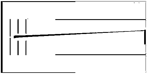
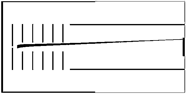
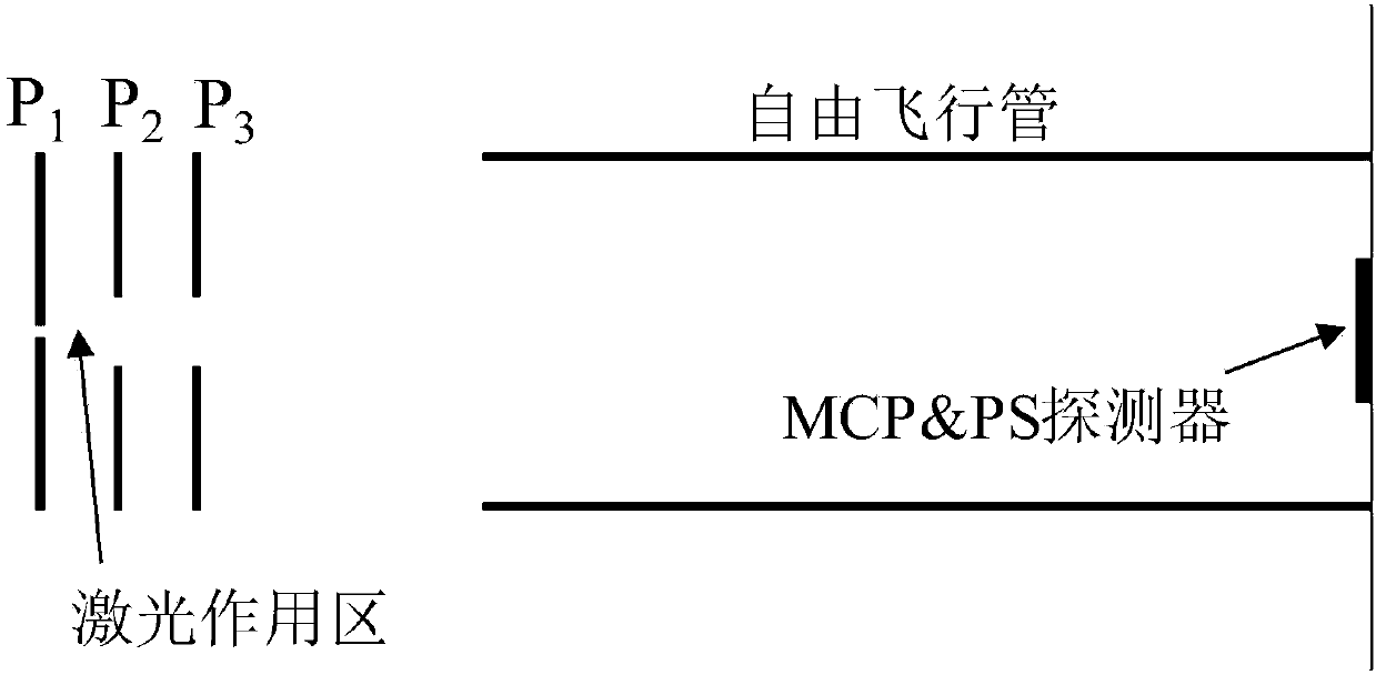
[0020] Please also see Figure 4 and Figure 5 , Figure 4 It is a schematic structural view of the low electric field optoelectronic imager provided by the present invention, Figure 5 Yes Yes Figure 4 The effect diagram of ...


PUM


Abstract

The invention provides a low electric field optoelectronic imager. The low electric field optoelectronic imager comprises a laser action zone, a free flight tube and a detector arranged sequentially in the moving direction of the charged particles. The laser action zone comprises at least four electrode plates arranged in parallel intervals and sequentially in the direction of movement of the charged particles. A potential difference is formed between every two adjacent electrode plates, and in the laser action zone, the potential differences share the identical direction. According to the invention, the low electric field optoelectronic imager keeps a low electric field in the measuring process by an instrument for the same total potential difference in prior art so that during the process of studying the action of light and matter, the electric field of the measuring instrument itself is greatly reduced, causing little change to the properties of the substance to be measured.

Description

technical field [0001] The invention relates to a low electric field photoelectron imager. Background technique [0002] The current low electric field optoelectronic imager was designed and invented by Dutch scientists Eppink and Parker in 1997. They designed three plates with round holes to form an ion lens under a certain optimized voltage configuration to achieve the same speed. But charged particles at different locations are focused and then collected by detectors at the back end of the flight tube, such as figure 1 shown. The settings of the three plates with round holes are as follows: P1 is the repelling plate, P2 is the accelerating plate, and P3 is the grounding plate. By changing the voltage of the repeller plate P1 and the accelerator plate P2, a focusing electric field based on the ion lens is formed, such as figure 2 shown. Under the action of ion lens, charged particles at different positions are focused on one point of the detector, which greatly improv...

Claims


Application Information

Patent Timeline
Patent Type & Authority Patents(China)
IPC IPC(8): H01J49/06H01J49/40
CPCH01J49/067H01J49/40
Inventor 刘玉柱肖韶荣夏俊荣苏静敖旷
Owner NANJING UNIV OF INFORMATION SCI & TECH
Why Eureka
Try Eureka