

Transparent material defect analysis method
A technology for transparent material and defect analysis, which is applied in the fields of material analysis using radiation, electrical components, semiconductor/solid-state device manufacturing, etc. Difficult to obtain physical maps and other issues, to achieve ideal results, high accuracy, and easy analysis
- Summary
- Abstract
- Description
- Claims
- Application Information
AI Technical Summary
Problems solved by technology
Method used
Image

Examples
Embodiment Construction
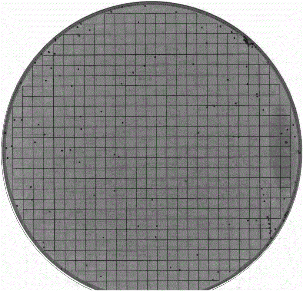
[0022] The defect analysis method of a transparent material in this embodiment first provides a transparent material to be analyzed, conducts microscopic defect detection on the transparent material to obtain a defect distribution map, and then attaches the transparent material to the defect distribution map through alignment , use the scanner to scan the image to obtain the object-result comparison chart, and analyze the correlation between the defect and the appearance of the transparent material through the object-result comparison chart.
[0023] The micro-defect detection of transparent materials is to scan the surface of transparent materials by laser, and obtain the specific distribution of various micro-defects by detecting scattering intensity, shape change, surface reflectivity and phase migration, etc. Matched defect distribution map. The defect distribution map is preferably a coordinate map, which is arranged by latitude and longitude lines and vertically intersec...
PUM
| Property | Measurement | Unit |
|---|---|---|
| Thickness | aaaaa | aaaaa |
Abstract
Description
Claims
Application Information