LED chip and its manufacturing method

A technology of LED chips and manufacturing methods, applied in electrical components, circuits, semiconductor devices, etc., can solve the problems of poor brightness of LED chips and difficult to emit light, so as to improve the brightness, reduce the probability of total reflection, and increase the probability of light emission. Effect

Inactive Publication Date: 2016-10-26
FOCUS LIGHTINGS SCI & TECH
View PDF3 Cites 0 Cited by
  • Summary
  • Abstract
  • Description
  • Claims
  • Application Information

AI Technical Summary

Problems solved by technology

In this case, light is prone to total reflection inside the LED chip, and it is not easy to emit light, and the brightness of the LED chip is not good.

Method used


Image

  • LED chip and its manufacturing method
  • LED chip and its manufacturing method
  • LED chip and its manufacturing method

Examples


Embodiment Construction

[0045] In order to enable those skilled in the art to better understand the technical solutions in the present invention, the technical solutions in the embodiments of the present invention will be clearly and completely described below in conjunction with the drawings in the embodiments of the present invention. Obviously, the described The embodiments are only some of the embodiments of the present invention, not all of them. Based on the embodiments of the present invention, all other embodiments obtained by persons of ordinary skill in the art without making creative efforts shall fall within the protection scope of the present invention.

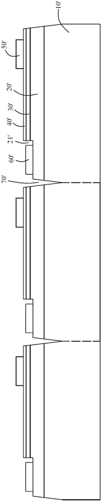
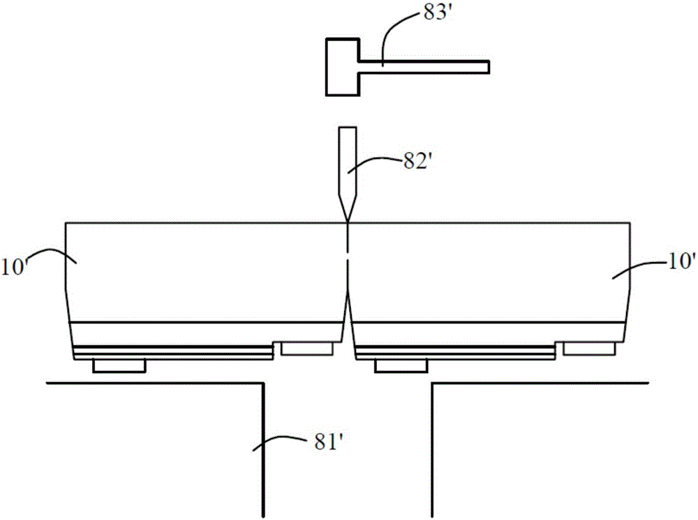
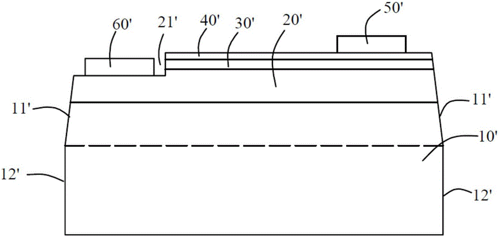
[0046] ginseng Image 6 Shown is a schematic cross-sectional structure diagram of the LED chip in the first embodiment of the present invention, and the LED chips are as follows from bottom to top:

[0047] Substrate 10, the substrate can be sapphire, Si, SiC, GaN, ZnO, etc., preferably, in this embodiment, a sapphire substrate is used...


PUM


Abstract

The present invention provides an LED chip and its manufacturing method. The LED chip comprises a substrate, a semiconductor epitaxial structure on the substrate, and a P-electrode and an N-electrode on the semiconductor epitaxial structure. The substrate comprises an upper substrate and a lower substrate. The cross section of the upper substrate is an isosceles trapezoid. The two sides of the upper substrate are referred to as first symmetrical slopes. The cross-section of the lower substrate is a parallelogram. The two sides of the lower substrate are referred to second parallel slops. The two sides of the semiconductor epitaxial structure are inclined along the first slopes of the upper substrate. According to the invention, the brightness of an LED chip improves under the premise that the splitting position is not changed to change the topography of a substrate and that the splitting rate is not compromised.

Description

technical field [0001] The invention relates to the technical field of LEDs, in particular to an LED chip and a manufacturing method thereof. Background technique [0002] A light-emitting diode (Light-Emitting Diode, LED) is a semiconductor electronic component that can emit light. This electronic component appeared as early as 1962. In the early days, it could only emit red light with low luminosity. Later, other monochromatic light versions were developed. Today, the light that can be emitted has covered visible light, infrared rays and ultraviolet rays, and the luminosity has also increased to a considerable extent. of luminosity. And the use is also used as indicator lights, display panels, etc. from the beginning; with the continuous advancement of technology, light-emitting diodes have been widely used in displays, TV lighting decoration and lighting. [0003] The LED chip manufacturing process in the prior art is as follows: [0004] ginseng figure 1 As shown, a ...

Claims


Application Information

Patent Timeline
Patent Type & Authority Applications(China)
IPC IPC(8): H01L33/20H01L33/00
CPCH01L33/20H01L33/005
Inventor 李庆王磊张广庚陈立人
Owner FOCUS LIGHTINGS SCI & TECH
Why Eureka
Try Eureka