Patterned sapphire substrate combining laser etching misplaced hemisphere and ODRs (Omni-directional Reflectors) and preparation method

A sapphire substrate, laser etching technology, applied in the field of optoelectronics, can solve problems such as unfavorable light extraction, and achieve the effects of improving light extraction efficiency, easy control of patterns, and increased light extraction opportunities

Pending Publication Date: 2018-07-10
Shandong Huaguang Optoelectronics Co. Ltd.
View PDF12 Cites 2 Cited by
  • Summary
  • Abstract
  • Description
  • Claims
  • Application Information

AI Technical Summary

Problems solved by technology

The patent is a triangular pyramid or triangular truncated figure to improve product quality and light output, but the area outside the figure is flat, which is not conducive to light output

Method used


Image

  • Patterned sapphire substrate combining laser etching misplaced hemisphere and ODRs (Omni-directional Reflectors) and preparation method
  • Patterned sapphire substrate combining laser etching misplaced hemisphere and ODRs (Omni-directional Reflectors) and preparation method
  • Patterned sapphire substrate combining laser etching misplaced hemisphere and ODRs (Omni-directional Reflectors) and preparation method

Examples


Embodiment 1

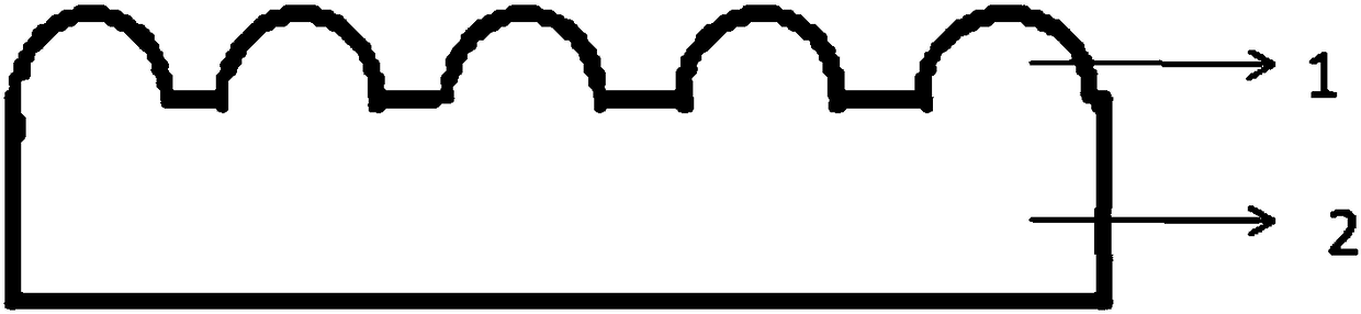
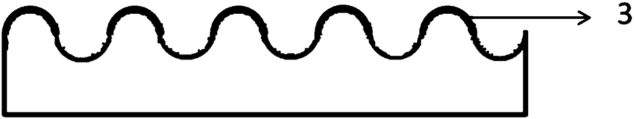
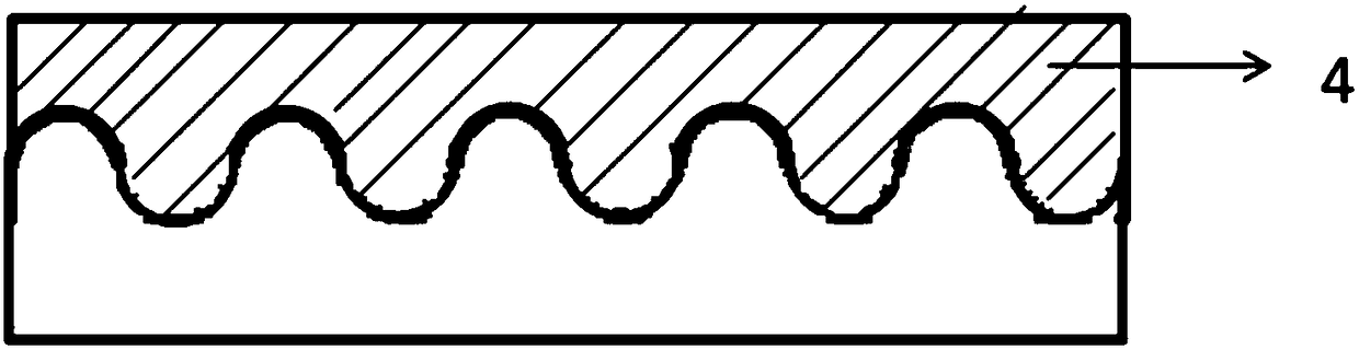
[0042] A sapphire pattern substrate combined with laser etching dislocation hemispheres and ODR, the substrate surface is provided with hemispherical protrusions, the substrate between two adjacent hemispherical protrusions is provided with hemispherical grooves, and the diameter of the hemispherical protrusions is 5 μm, the distance between two adjacent hemispherical protrusions is 5 μm; the surface of the hemispherical protrusions is provided with a mirror layer, and the mirror layer is TiO 2 / SiO 2 layer, the thickness of the mirror layer is 200nm.

[0043] Among them, TiO 2 / SiO 2 The layers are alternately grown SiO 2 layer and TiO 2 layer, the alternating repetition period is 1, that is, a SiO2 layer+TiO2 layer is alternately grown. Alternately grown SiO in 1 alternate repeating cycle 2 layer thickness of 100 nm, alternately grown TiO 2 The layer thickness was 100 nm.

Embodiment 2

[0045] A sapphire pattern substrate combined with laser etching dislocation hemispheres and ODR, its structure is as described in Example 1, the difference is that the diameter of the hemispherical protrusions is 1 μm, and the distance between two adjacent hemispherical protrusions is 1 μm.

Embodiment 3

[0047] A sapphire pattern substrate combined with laser etching dislocation hemisphere and ODR, its structure is as described in embodiment 1, the difference is that the mirror layer is Au 2 O / SiO 2 layer.


PUM


Abstract

The invention relates to a patterned sapphire substrate combining laser etching misplaced hemispheres and ODRs (Omni-directional Reflectors) and a preparation method, and belongs to the field of optoelectronic technologies. According to the invention, misplaced hemispherical protrusions are formed on the sapphire substrate through laser etching, the single graphical structure of the patterned sapphire substrate is hemispherical, and the oblique side wall of each hemispherical protrusion is provided with a reflector layer. The misplaced hemispherical protrusions are formed on the basis of the sapphire substrate, laser etching is performed, the precision is high, the pattern is easy to control, the light emitting opportunity is increased, and the light emitting efficiency is greatly improved. Meanwhile, the ODRs are prepared on the upper hemispherical patterns of the patterned sapphire substrate, and then a GaN layer grows epitaxially at the surfaces of the ODRs, thereby not only being capable of suppressing the extension of defects, but also being capable of improving the crystal quality of GaN, and improving the light emitting efficiency at the same time.

Description

technical field [0001] The invention relates to a sapphire pattern substrate combined with laser etching dislocation hemispheres and ODR and a preparation method thereof, belonging to the field of optoelectronic technology. Background technique [0002] The epitaxial layer of GaN-based materials is mainly grown on the sapphire substrate. The sapphire substrate has many advantages: first, the production and application of the sapphire substrate is mature and the quality is good; second, the sapphire has good stability and can be used in high temperature During the growth process; finally, sapphire has high mechanical hardness and is easy to handle and clean. Because most GaN-LEDs are grown on sapphire substrates, there are many problems in growing GaN materials on sapphire substrates. The biggest problem is surface light emission. Problem, although GaN-based LEDs have been industrialized, the problem of low light output efficiency of chips has not been well resolved. Accordi...

Claims


Application Information

Patent Timeline
Patent Type & Authority Applications(China)
IPC IPC(8): H01L33/20H01L33/10H01L33/00H01L21/268
CPCH01L33/007H01L33/10H01L33/20H01L21/268
Inventor 邵慧慧徐现刚刘成成于果蕾李沛旭
Owner Shandong Huaguang Optoelectronics Co. Ltd.
Why Eureka
Try Eureka