A packaging structure that improves the brightness of vertical light-emitting diode chips

A light-emitting diode and packaging structure technology, which is applied in the direction of electrical components, circuits, semiconductor devices, etc., can solve the problems of reduced brightness, low production cost, and poor efficiency of blue light conversion to white light, etc., to achieve the effect of increasing light intensity and enhancing the probability of light output

Active Publication Date: 2016-01-27
QUANZHOU SANAN SEMICON TECH CO LTD
View PDF8 Cites 0 Cited by
  • Summary
  • Abstract
  • Description
  • Claims
  • Application Information

AI Technical Summary

Problems solved by technology

At present, front-mounted LED chips are the most widely used on the application side. Its advantage is that the production cost is low and the yield rate is high. Therefore, the use of front-mounted LED chips is more popular at present. Generally, it is a high-power light-emitting diode lamp bead, and the high-power front-mounted chip required by it can no longer be met. The development of vertical light-emitting diode chips has emerged as the times require. The vertical electrode design makes the vertical light-emitting diode chips can withstand large power usage, and can generally be used The power of LED chip is about 1.5 times that of the formal LED chip. However, due to the design of the vertical electrode, the vertical LED chip must also use a conductive substrate. Considering the cost performance, the silicon substrate becomes an ideal choice.
[0003] Traditional silicon substrate LED vertical chip packaging structure, such as figure 1 As shown, the blue light provided by the light-emitting diode chip and the blue light enters the encapsulant to excite yellow light, and the blue light and the yellow light are mixed to produce white light. In the process of blue light entering the encapsulant particle, the encapsulant particle will only absorb part of the blue light. , and the remaining blue light will be refracted into the next encapsulation particle, so the blue light will be continuously refracted to change the light path during a series of light mixing processes, and even some blue light will be reflected back to the chip, because the silicon substrate will All light in the range of visible light is absorbed, especially blue light and yellow light in the visible range have a certain absorption rate, so when vertical light-emitting diodes are used in lighting systems, such as sealed into LED lamp beads, it will cause blue light to be converted to white light Efficiency gets worse and its brightness drops

Method used


Image

  • A packaging structure that improves the brightness of vertical light-emitting diode chips
  • A packaging structure that improves the brightness of vertical light-emitting diode chips
  • A packaging structure that improves the brightness of vertical light-emitting diode chips

Examples


Embodiment 1

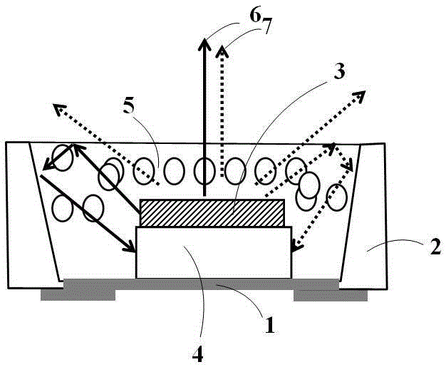
[0028] see figure 2 As shown, a packaging structure for improving the brightness of vertical light-emitting diode chips in this embodiment includes a bracket system, which is mainly used to carry the LED vertical chip 3 on the silicon substrate. The metal support 1 of the structure 8, the function of the metal support 1 is for electrode conduction and heat dissipation, and the function of the surrounding baffle structure 8 is to reduce or prevent the light reflected by the LED vertical chip 3 from being absorbed by the silicon substrate 4, and to absorb it The packaging structure is reflected, in which the height of the surrounding baffle is equal to the substrate thickness of the silicon substrate LED chip; the plastic cup 2 is connected to the periphery of the bracket system, and the shape of the plastic cup can be adjusted according to the need to control the light shape; the silicon substrate LED chip passes through The die-bonding method is placed on the support system; ...

Embodiment 2

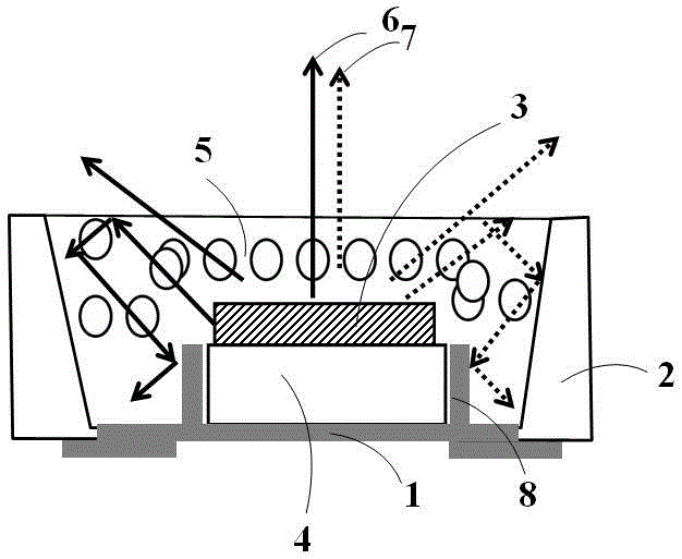
[0032] see image 3 As shown, another packaging structure for improving the brightness of the vertical light-emitting diode chip in this embodiment includes a support system, which is mainly used to carry the silicon substrate LED vertical chip 4, and the support system consists of a metal support 1 and a surrounding type The baffle plate 8 is composed of two separate parts. The metal frame 1 is made of metal materials. The function of the metal frame 1 is for electrode conduction and heat dissipation. The function of the surrounding baffle structure 8 is to reduce or prevent the reflection of the LED chip. The light is absorbed by the silicon substrate and reflected out of the packaging structure, wherein the height of the surrounding baffle is greater than 1 / 2 of the substrate thickness of the silicon substrate LED chip and less than the substrate thickness of the silicon substrate LED chip; the plastic cup 2 and the bracket The periphery of the system is connected, and the ...

Embodiment 3

[0036] The difference from Embodiment 1 is that the packaging structure for improving the brightness of the vertical light-emitting diode chip in this embodiment, in which there is a gap between the substrate of the silicon substrate LED chip and the surrounding baffle, is filled with reflective materials, such as White glue (mirror ink), which can further enhance the reflection of blue light and yellow light that would have been absorbed by the silicon substrate, thereby further improving the light intensity of the vertical light-emitting diode chip.


PUM


Abstract

The invention provides a packaging structure for vertical light-emitting diode chip brightness, which at least includes a bracket system, a plastic cup connected to the outer periphery of the bracket system, an LED chip containing a light-absorbing substrate placed on the bracket system, and the packaging glue is distributed on the LED The outer periphery of the chip is characterized in that it also includes a baffle that surrounds the outer side wall of the light-absorbing substrate. By adding a baffle structure to the bracket system of the packaging structure, the light that would otherwise be absorbed by the light-absorbing substrate can be effectively avoided and reflected out of the packaging structure, thereby enhancing the probability of light extraction and thereby increasing the light intensity of the vertical light-emitting diode chip.

Description

technical field [0001] The invention relates to a packaging structure for improving the brightness of a vertical light-emitting diode chip, which reduces or avoids the light absorption of the substrate of the vertical chip through the design of the bracket, and improves the packaging brightness, belonging to the field of light-emitting diodes. Background technique [0002] Light-emitting diode chips can be roughly divided into three categories according to their structure, namely front-mounted light-emitting diode chips, flip-chip light-emitting diode chips, and vertical light-emitting diode chips. At present, front-mounted LED chips are the most widely used on the application side. Its advantage is that the production cost is low and the yield rate is high. Therefore, the use of front-mounted LED chips is more popular at present. Generally, the lamp beads of high-power light-emitting diodes cannot meet the requirements of high-power front-mounted chips, so the development o...

Claims


Application Information

Patent Timeline
Patent Type & Authority Patents(China)
IPC IPC(8): H01L33/52
CPCH01L33/56H01L33/486H01L33/60
Inventor 赵志伟江彦志
Owner QUANZHOU SANAN SEMICON TECH CO LTD
Why Eureka
Try Eureka