Anisotropic conductive film and its preparation method
- Summary
- Abstract
- Description
- Claims
- Application Information
AI Technical Summary
Problems solved by technology
Method used
Image
Examples
preparation example Construction
[0087] >
[0088] Next, an example of the production method of the anisotropic conductive film of the present invention will be described.
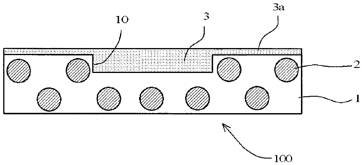
[0089] The anisotropic conductive film of the present invention can be produced by performing a low-adhesion region forming process on a part of one surface of the insulating adhesive layer. Examples of the low-adhesive region forming process include pouring a low-adhesive region-forming material and performing smoothing by a known method; raster processing with a laser; or micro-concave-convex processing by photolithography.
[0090] A preferred example of the production method of the anisotropic conductive film of the present invention is a production method having the following steps (A) to (C). Each process is described below.
[0091] Process (A)
[0092] First, a composition for forming an insulating adhesive layer containing conductive particles is applied on a mold having convex portions corresponding to low-adhesive regions, a...
Embodiment 1~5
[0103] With toluene, 60 parts by mass of phenoxy resin (YP-50, Nippon Steel Sumikin Chemical Co., Ltd.), 40 parts by mass of acrylate (EP600, Daicel-Allnex Ltd. (Daicel-Allnex Ltd. (Daycel Aurnex))), 2 parts by mass of photoradical polymerization initiator (IRGACURE 369, Mitsubishi Chemical Co., Ltd.) and 10 parts by mass of conductive particles (Ni / Au plated resin particles, AUL704, Sekisui Chemical Industry Co., Ltd.) with an average particle diameter of 4 μm ) to prepare a mixed solution so that the resin solid content is 50% by mass.
[0104] Using this mixed solution and forming the predetermined protrusions (in the case of Examples 1 to 4, the same Figure 4 The mode of corresponding continuous extending setting, under the situation of embodiment 5 is and Figure 5 Corresponding to the sheet-shaped mold in a discontinuous stepping stone shape), an insulating adhesive layer having a width of 2 mm was prepared after cutting. The insulating adhesive layer was removed from...
Embodiment 6
[0108] (Preparation of Insulating Adhesive Layer Arranged with Conductive Particles)
[0109] With toluene, 60 parts by mass of phenoxy resin (YP-50, Nippon Steel & Sumikin Chemical Co., Ltd.), 40 parts by mass of acrylate (EP600, Daicel-Allnex Ltd. (Daicel-Allnex Ltd. (Daycel Allnex Co., Ltd.)) and 2 parts by mass of a photoradical polymerization initiator (IRGACURE 369, Mitsubishi Chemical Co., Ltd.) prepared a mixed liquid so that the solid content would be 50% by mass. The mixed solution was coated on a polyethylene terephthalate film having a thickness of 50 μm so that the dry thickness would be 8 μm, and dried in an oven at 80° C. for 5 minutes to form a photoradically polymerizable resin layer.
[0110] Next, in the obtained photoradically polymerizable resin layer, conductive particles (Ni / Au plated resin particles, AUL704, Sekisui Chemical Co., Ltd.) having an average particle diameter of 4 μm were arranged in a single layer at a distance of 4 μm. Furthermore, from t...
PUM
| Property | Measurement | Unit |
|---|---|---|
| height | aaaaa | aaaaa |
| adhesion strength | aaaaa | aaaaa |
| glass transition temperature | aaaaa | aaaaa |
Abstract
Description
Claims
Application Information


