
Method for preparing copper-bismuth-sulfur film

A copper-bismuth-sulfur, thin-film technology, applied in ion implantation plating, metal material coating process, coating and other directions, can solve the problems of poor crystalline properties of semiconductor materials, electrical properties that cannot reach photovoltaic cells, and poor sample uniformity. , to achieve the effect of environmental protection process method, less impurity content and good film flatness

Inactive Publication Date: 2016-11-09
BEIJING INSTITUTE OF TECHNOLOGYGY
View PDF5 Cites 2 Cited by
  • Summary
  • Abstract
  • Description
  • Claims
  • Application Information

AI Technical Summary

Problems solved by technology

Pyrolysis spray method and chemical water bath deposition method will introduce a large amount of impurities, resulting in poor crystallization performance of semiconductor materials on the one hand, and on the other hand, the electrical properties cannot meet the requirements of photovoltaic cells
Both the reactive sputtering method and the co-evaporation method are vacuum coating methods, which can obtain high-quality films, but both require high equipment control, such as adjusting the ratio of elements, controlling the reaction atmosphere, etc.
Electrodeposited films are generally relatively pure, but electrodeposition is subject to the control of electric field distribution, and the prepared samples have poor uniformity

Method used

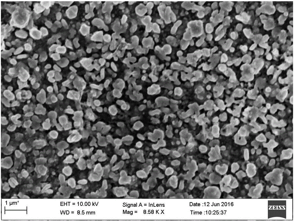
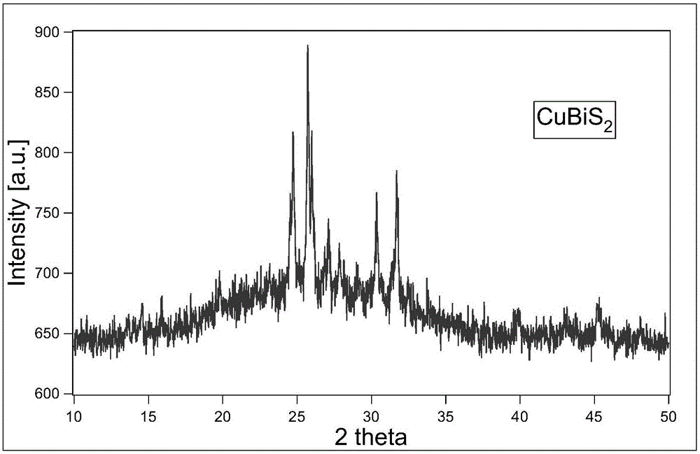
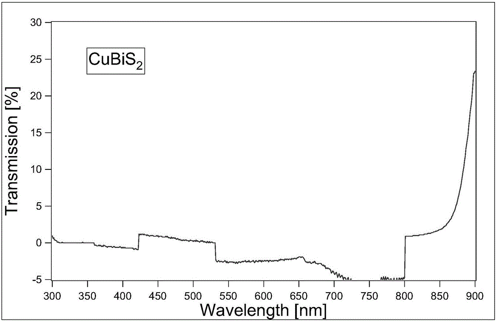

Image

  • Method for preparing copper-bismuth-sulfur film
  • Method for preparing copper-bismuth-sulfur film
  • Method for preparing copper-bismuth-sulfur film

Examples


Embodiment 1

[0039] A method for preparing copper-bismuth-sulfur thin films, the method steps are as follows:

[0040] Step 1. Put the glass with a thickness of 2mm into the mixed solution prepared by micro-90 and deionized water at a mass ratio of 1:50, then heat it to 70°C, keep it for 15 minutes, continue to heat up to 90°C, and ultrasonically clean it for 15 minutes , take out the glass and rinse it with deionized water for 5 times, and then use N 2 blow dry glass;

[0041] Step 2. Vacuum evaporation metal bismuth thin film and CuS thin film

[0042] Put the glass on the stage in the vacuum evaporation device, set the speed of the stage to 10r / min, and control the chamber pressure of the vacuum evaporation device at 1×10 -5 Pa~5×10 -2 Within the range of Pa, turn on the power of the bismuth evaporation source to heat the bismuth evaporation source to 280°C, then open the baffle on the stage to start the evaporation of metal bismuth, measured by the crystal oscillator film thickness ...

Embodiment 2

[0046] A method for preparing copper-bismuth-sulfur thin films, the method steps are as follows:

[0047] Step 1. Put the glass with a thickness of 4mm into the mixed solution prepared by micro-90 and deionized water at a mass ratio of 1:50, then heat it to 60°C, keep it for 30 minutes, then continue to heat up to 80°C, and ultrasonically clean it for 30 minutes , take out the glass and rinse it three times with deionized water, and then use N 2 blow dry glass;

[0048] Step 2. Vacuum evaporation metal bismuth thin film and CuS thin film

[0049] Put the glass on the stage in the vacuum evaporation device, set the speed of the stage to 10r / min, and control the chamber pressure of the vacuum evaporation device at 1×10 -5 Pa~5×10 -2 Within the range of Pa, turn on the power of the bismuth evaporation source to heat the bismuth evaporation source to 300°C, then open the baffle on the stage to start the evaporation of metal bismuth, measured by the crystal oscillator film thick...

Embodiment 3

[0053] A method for preparing copper-bismuth-sulfur thin films, the method steps are as follows:

[0054] Step 1. Put the glass with a thickness of 1mm into the mixed solution prepared by micro-90 and deionized water at a mass ratio of 1:50, then heat it to 60°C, keep it for 30min, then continue to heat up to 90°C, and ultrasonically clean it for 15min , took out the glass and rinsed it four times with deionized water, and then washed it with N 2 blow dry glass;

[0055] Step 2. Vacuum evaporation metal bismuth thin film and CuS thin film

[0056] Put the glass on the stage in the vacuum evaporation device, set the speed of the stage to 10r / min, and control the chamber pressure of the vacuum evaporation device at 1×10 -5 Pa~5×10 -2 Within the range of Pa, turn on the power of the bismuth evaporation source to heat the bismuth evaporation source to 300°C, then open the baffle on the stage to start the evaporation of metal bismuth, measured by the crystal oscillator film thic...


PUM

PropertyMeasurementUnit
thicknessaaaaaaaaaa
lengthaaaaaaaaaa
widthaaaaaaaaaa

Abstract

The invention relates to a method for preparing a copper-bismuth-sulfur film, and belongs to the field of semiconductor materials. Firstly, a metal bismuth film is evaporated and plated on a clean substrate in vacuum; then, a CuS film is evaporated and plated on the metal bismuth film in vacuum; finally, the substrate deposited with the metal bismuth film and the CuS film is put in a heating furnace for heat treatment; and the film deposited on the substrate is the copper-bismuth-sulfur film. The method performs the film plating and the vulcanization under the vacuum condition to guarantee the material purity; the ratios of elements in the prepared film are controlled through the film plating thickness; the film crystallization conditions are controlled through the vulcanization treatment temperature and the sulfur atmosphere, so that the control is simpler; and elementary sulfur, not hydrogen sulfide is adopted in vulcanization, so that the method is more environment-friendly.

Description

technical field [0001] The invention relates to a method for preparing a copper-bismuth-sulfur thin film, which belongs to the field of semiconductor materials. Background technique [0002] Solar energy is a clean, non-polluting, inexhaustible renewable energy, and does not produce any environmental pollution, so it is favored by people. Among the effective utilization of solar energy, solar photovoltaic utilization is the fastest growing and most dynamic research field in recent years, for which people have developed and developed solar cells. Solar cells are mainly based on semiconductor materials, which convert solar energy into electrical energy by utilizing the photoelectric conversion effect after absorbing light. Under the action of the p-n junction electric field, the photogenerated holes flow from the n region to the p region, and the photogenerated electrons flow from the p region to the n region, forming a photocurrent. [0003] Thin-film compound solar cells h...

Claims


Application Information

Patent Timeline
Patent Type & Authority Applications(China)
IPC IPC(8): C23C14/06C23C14/18C23C14/24C23C14/58
CPCC23C14/0623C23C14/18C23C14/24C23C14/5806
Inventor 韩俊峰刘雨浓姚裕贵
Owner BEIJING INSTITUTE OF TECHNOLOGYGY
Learn More