Photoelectric electric field near-field probe made by printed circuit board

A printed circuit board and near-field probe technology, applied in the field of measurement probes, can solve the problems of large probe size, narrow probe frequency measurement range, and probe easily interfered, achieving the effect of clear design ideas and excellent measurement range

Inactive Publication Date: 2018-08-17
HEBEI UNIV OF TECH
View PDF9 Cites 0 Cited by
  • Summary
  • Abstract
  • Description
  • Claims
  • Application Information

AI Technical Summary

Problems solved by technology

[0004] The technical problem to be solved by the present invention is to provide a photoelectric electric field near-field probe made by using a printed circuit board, which is a miniature receiving antenna using a strip line and a micro-bandgap structure made by using a printed circuit board. The power-adjusted laser adjusts the capacitance parameters of the probe circuit, which overcomes the shortcomings of the existing electric field near-field probes that are susceptible to interference, narrow probe frequency measurement range and large probe size

Method used


Image

  • Photoelectric electric field near-field probe made by printed circuit board
  • Photoelectric electric field near-field probe made by printed circuit board
  • Photoelectric electric field near-field probe made by printed circuit board

Examples


Embodiment

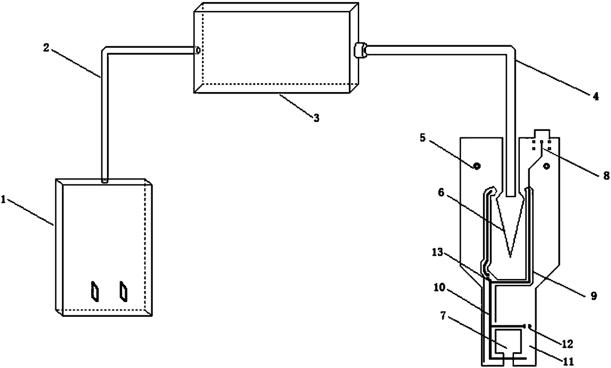
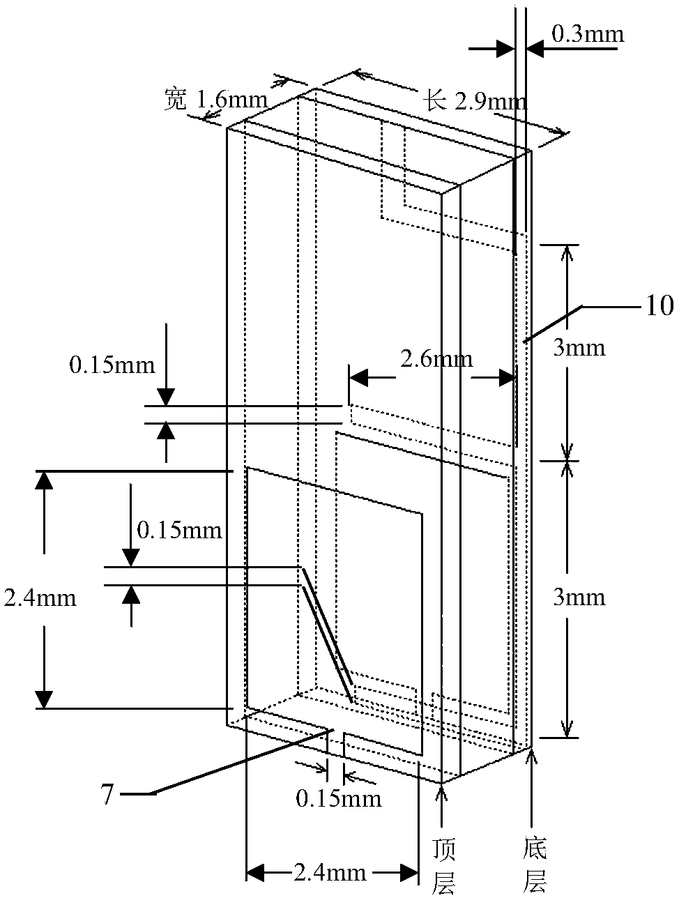
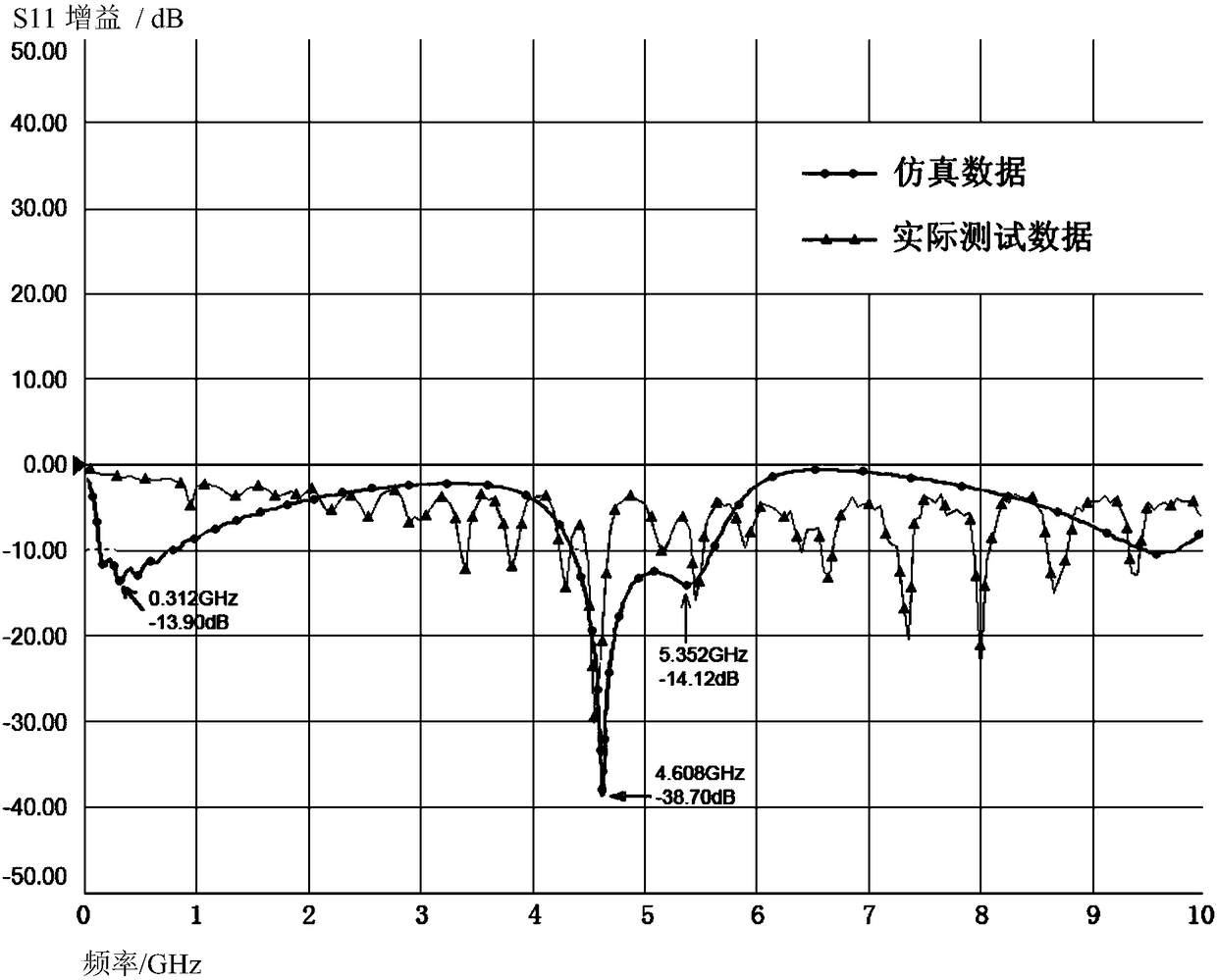
[0041] The photoelectric electric field near-field probe made by the printed circuit board in this embodiment is a miniature receiving antenna made by the printed circuit board with a strip line and micro band gap structure. figure 1 The assembly structure of the illustrated embodiment includes an adjustable power supply 1, a cable 2, a laser 3, a black optical cable 4, a fixing hole 5, a silicon photocell array 6, a micro band gap structure 7, a signal output terminal 8, a signal line shield 9 , Strip line 10, copper-clad ground 11, compensation capacitor 12 and current-limiting resistor 13; the connection method of the above components is: adjustable power supply 1 supplies power to laser 3 through cable 2, and the laser light emitted by laser 3 is transmitted through black fiber optic cable 4. To the silicon photovoltaic cell array 6, the silicon photovoltaic cell array 6 converts lasers of different powers into electrical energy and forms different voltages, and the subsequen...


PUM


Abstract

The invention relates to a photoelectric electric field near field probe manufactured by using a printed circuit board and relates to a measuring probe for measuring an electromagnetic variable. The photoelectric electric field near field probe comprises an adjustable power supply, a cable, a laser, a black skin optical cable, a fixing hole, a silicon photocell array, a microstrip gap structure, a signal output terminal, a signal line shield, a band-shaped line, a copper-clad ground, a compensation capacitor, and a current-limiting resistor. The photoelectric electric field near field probe is a micro receiving antenna manufactured by using the printed circuit board and provided with the band-shaped line and the microstrip gap structure. The capacitor parameter of a probe circuit is adjusted by a power-adjustable laser so that a defect is overcome that a conventional electric field near field probe is susceptible to interference, narrow in frequency measurement range, and large in size.

Description

Technical field [0001] The technical scheme of the present invention relates to a measuring probe for measuring electromagnetic variables, specifically, a photoelectric electric field near-field probe made by a printed circuit board. Background technique [0002] The rapid development of electronic technology and electromagnetic compatibility has led to the advancement of electronic measurement technology. The electromagnetic compatibility and radiation problems of various electronic devices have become increasingly prominent. New technologies and equipment for near-field detection of electric fields are emerging in endlessly, as the core of near-field electric field measurement Components, the performance parameters of the electric field near-field probe become the key to restrict the entire electric field measurement system, and its measurement frequency range, sensitivity and accuracy are the main determinants. In order to adapt to a wider frequency range, existing electric fi...

Claims


Application Information

Patent Timeline
Patent Type & Authority Patents(China)
IPC IPC(8): G01R29/08
CPCG01R29/0814G01R29/0885
Inventor 李尔平宋涛
Owner HEBEI UNIV OF TECH
Why Eureka
Try Eureka