Device and method for pulse laser etching of conducting film layer on double-sided indium tin oxide (ITO) glass

A pulsed laser, conductive film technology, applied in laser welding equipment, welding equipment, metal processing equipment and other directions, can solve the problems of small tension value, low yield, complex process, etc., to achieve linear stability, complete functions, Overcome the effects of system complexity

Inactive Publication Date: 2012-02-22
SUZHOU DELPHI LASER
View PDF5 Cites 30 Cited by
  • Summary
  • Abstract
  • Description
  • Claims
  • Application Information

AI Technical Summary

Problems solved by technology

[0004] The width of the double-sided conductive film layer on the traditional wet-etched touch screen can only reach 80um, and the yield rate is low, the linearity is uneven, and it is cumbersome to replace different batches of products. It needs to be cleaned with chemical medicine, which pollutes the environment;...

Method used


Image

  • Device and method for pulse laser etching of conducting film layer on double-sided indium tin oxide (ITO) glass
  • Device and method for pulse laser etching of conducting film layer on double-sided indium tin oxide (ITO) glass

Examples


Embodiment Construction

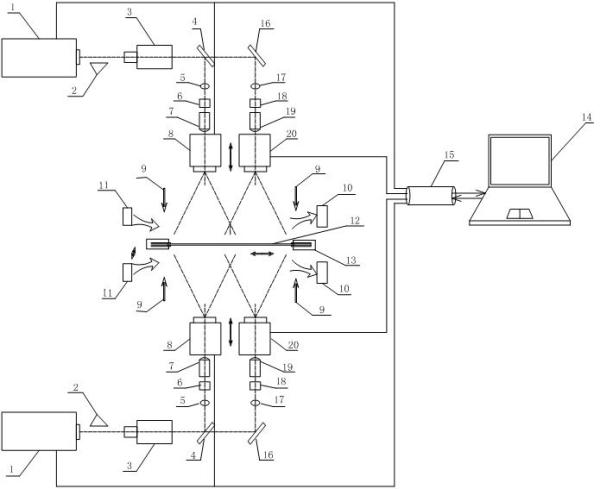
[0014] Such as figure 1 As shown, the pulse laser etching device for the conductive film layer on double-sided ITO glass, the film material 12 is clamped and fixed by the clamping cylinder 13, and a set of the same pulse laser etching device is arranged on the front and back of the film material 12, so Each set of pulse laser etching device includes a high-frequency short-pulse laser 1, a beam expander 3, a half-mirror 4, a Glan prism 6, and a full-reflection mirror 16. The high-frequency short-pulse laser 1 has a wavelength of 190nm~ 1100nm, pulse width 1ps ~ 200ns, frequency 10KHz ~ 100MHz laser, the output end of the high frequency short pulse laser 1 is arranged with an optical gate 2, the output end of the optical gate 2 is provided with a beam expander 3, the beam expander 3 The output end is arranged with a half-mirror 4, the output end of the half-mirror 4 is arranged with a first 1 / 2 wave plate 5 and a full reflection mirror 16, and the output end of the first 1 / 2 wav...


PUM

PropertyMeasurementUnit
Wavelengthaaaaaaaaaa
Pulse widthaaaaaaaaaa

Abstract

The invention relates to a device and a method for the pulse laser etching of a conducting film layer on double-sided indium tin oxide (ITO) glass. The front and back surfaces of a film material are provided with a set of pulse laser etching device respectively. Each set of pulse laser etching device comprises a high-frequency short-pulse laser, a semi-transmitting semi-reflecting mirror, a Glan prism and a completely reflecting mirror; the output end of the high-frequency short-pulse laser is sequentially provided with an optical gate, a beam expander and the semi-transmitting semi-reflecting mirror; the output end of the semi-transmitting semi-reflecting mirror is provided with a first 1/2 wave plate and the completely reflecting mirror; the output end of the first 1/2 wave plate is sequentially provided with a first Glan prism and a first three-dimensional (3D) dynamic focusing lens; the output end of the first 3D dynamic focusing lens is provided with a first galvanometer; the output end of the completely reflecting mirror is provided with a second 1/2 wave plate; the output end of the second 1/2 wave plate is sequentially provided with a second Glan prism and a second 3D dynamic focusing lens; the output end of the second 3D dynamic focusing lens is provided with a second galvanometer; and the output ends of the first and second galvanometers are both dead against the surface of the film material. The device and the method are used for etching double-sided ITO glass in different touch screen products to realize high-efficiency high-accuracy circuit manufacturing.

Description

technical field [0001] The invention relates to a device and a method for pulse laser etching a conductive film layer on double-sided ITO glass, and belongs to the technical field of laser micromachining. Background technique [0002] Traditionally, there are two methods of manufacturing lines on the double-sided conductive film layer on the touch screen: chemical wet etching and yellow photolithography. Among them, in the process method of chemical wet etching conductive film layer, the process design takes a long time to complete the etching, and the cost of fixtures and consumables needs to be invested. The pollution is more serious, and the energy waste of the whole technological process is more serious. However, the yellow photolithography process requires a large initial investment and high cost. The selectivity of materials is relatively narrow, and it is not suitable for all the production methods of conductive film layers on the market. In addition, the daily maint...

Claims


Application Information

Patent Timeline
IPC IPC(8): B23K26/36B23K26/067B23K26/14B23K26/362
Inventor 赵裕兴狄建科张伟
Owner SUZHOU DELPHI LASER
Why Eureka
Try Eureka