Highly sensitive magnetic sensor and its manufacturing method

A technology of a magnetic sensor and a manufacturing method, which is applied in the directions of instruments, measuring magnetic variables, and single-equipment manufacturing, can solve the problem of increasing the distance between the magnetic induction film 14 and the measured medium, reducing the sensitivity and consistency of the magnetic sensor, and reducing the yield of the magnetic sensor. and other problems, to achieve the effect of shortening the distance, improving the yield and improving the processing efficiency

Inactive Publication Date: 2019-06-04
BEIJING JIAYUE TONGLEJI ELECTRONICS
View PDF5 Cites 0 Cited by
  • Summary
  • Abstract
  • Description
  • Claims
  • Application Information

AI Technical Summary

Problems solved by technology

Since the chip pad 15 is arranged on the upper surface of the substrate 13, when the gold wire 17 is electrically connected to the chip pad 15, the top of the gold wire 17 is tens or even hundreds of microns higher than the top surface of the magnetic induction film 14, which increases the The distance between the magnetic induction film 14 and the measured medium reduces the sensitivity and consistency of the magnetic sensor
Moreover, the polishing of this magnetic sensor after packaging is easy to grind off the gold wire 17 or loosen the solder joints between the gold wire 17 and the chip pad 15, which reduces the yield of the magnetic sensor.

Method used


Image

  • Highly sensitive magnetic sensor and its manufacturing method
  • Highly sensitive magnetic sensor and its manufacturing method
  • Highly sensitive magnetic sensor and its manufacturing method

Examples


Embodiment Construction

[0037] In order to enable those skilled in the art to better understand the technical solution of the present invention, the highly sensitive magnetic sensor provided by the present invention will be described in detail below with reference to the accompanying drawings.

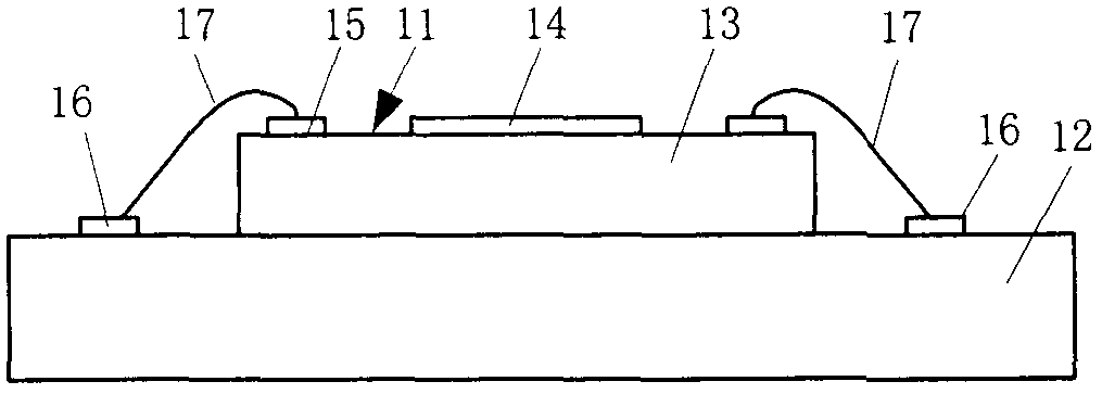
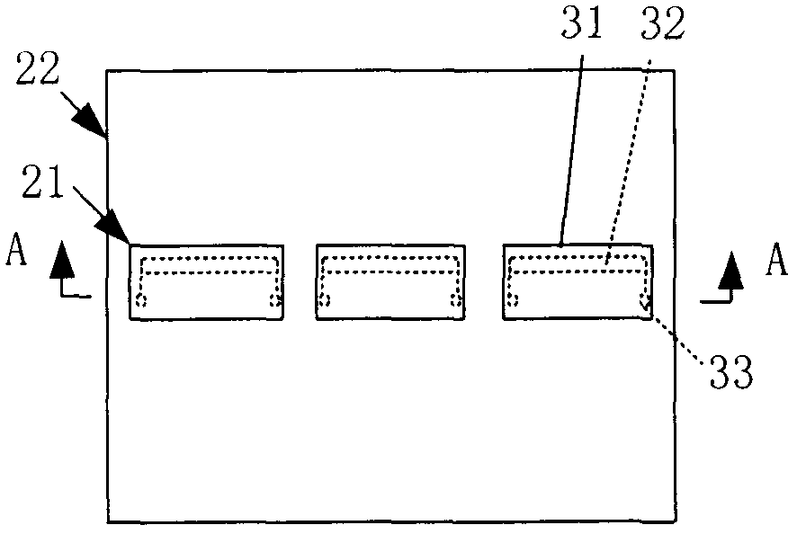
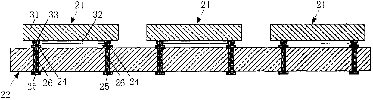
[0038] Such as figure 2 with image 3 As shown, the high-sensitivity magnetic sensor includes a chip 21 and a package substrate 22 , wherein the chip 21 is used to sense a magnetic mark disposed in the detected medium and output an induction signal. The packaging substrate 22 is used to support and fix the chip 21 and at the same time lead out the induction signal of the chip 21 . The magnetic sensor can be provided with one chip 21 or multiple chips 21 as required. When the magnetic sensor includes multiple chips 21 , the multiple chips 21 are arranged in a horizontal arrangement so as to completely cover the width direction of the magnetic sensor. In this embodiment, a magnetic sensor provided with thre...


PUM


Abstract

A high sensitivity magnetic sensor, comprising chips (21) and a package substrate (22); the chips (21) comprise substrates (31), and magnetic induction films (32) and chip bonding pads (33) disposed on the substrates (31); the magnetic induction films (32) are used to induce a magnetic field and output inductive signals, and the chip bonding pads (33) are correspondingly electrically connected to the magnetic induction films (32) as the input / output terminals of the chips (21); the magnetic induction films (32) and the chip bonding pads (33) are disposed on the same side of the substrates (31); the package substrate (22) is provided with conductive circuits (26) correspondingly electrically connected to the chip bonding pads (33); the surfaces of the chips (21) provided with the magnetic induction films (32) face and are layered on the package substrate (22); and the chip bonding pads (33) are correspondingly electrically connected to first substrate bonding pads (24) disposed on the surface of the package substrate (22). The high sensitivity magnetic sensor has good sensitivity and consistency, and has a simple manufacturing process and high yield of finished products.

Description

technical field [0001] The invention belongs to the field of precision measurement, and in particular relates to a high-sensitivity magnetic sensor and a manufacturing method thereof. Background technique [0002] Magnetic sensors are widely used in the fields of financial electronics, electric power and transportation, such as magnetic heads of banknote detectors in the financial field, card readers for mobile payment, etc. These application areas have high requirements on the sensitivity and consistency of magnetic sensors. [0003] figure 1 It is a structural schematic diagram of a relatively advanced magnetic sensor currently used for the magnetic head of a money detector. Such as figure 1 As shown, the magnetic sensor includes a chip 11 and a substrate 12. The chip 11 includes a substrate 13 and a magnetic induction film 14 and a chip pad 15 disposed on the surface of the substrate 13. The magnetic induction film 14 is used to induce a magnetic field and output an in...

Claims


Application Information

Patent Timeline
Patent Type & Authority Patents(China)
IPC IPC(8): G01R33/07G01R33/09G06K7/00G06K19/07
CPCG01R33/0052
Inventor 时启猛王春华
Owner BEIJING JIAYUE TONGLEJI ELECTRONICS
Why Eureka
Try Eureka