Manufacturing method for pixel defining layer and manufacturing method for OLED device

A pixel-defining layer and manufacturing method technology, applied in semiconductor/solid-state device manufacturing, electric solid-state devices, semiconductor devices, etc., can solve the problems that limit the large-scale commercialization of OLED displays and high manufacturing costs, and achieve good insulation and service life. Long, stable effect of OLED material

Active Publication Date: 2016-11-16
SHENZHEN CHINA STAR OPTOELECTRONICS TECH CO LTD
View PDF4 Cites 22 Cited by
  • Summary
  • Abstract
  • Description
  • Claims
  • Application Information

AI Technical Summary

Problems solved by technology

However, due to the high cost of vacuum thermal evaporation preparation, the large-scale commercialization of OLED displays is limited.

Method used


Image

  • Manufacturing method for pixel defining layer and manufacturing method for OLED device
  • Manufacturing method for pixel defining layer and manufacturing method for OLED device
  • Manufacturing method for pixel defining layer and manufacturing method for OLED device

Examples


Embodiment Construction

[0031] In order to further illustrate the technical means adopted by the present invention and its effects, the following describes in detail in conjunction with preferred embodiments of the present invention and accompanying drawings.

[0032] see figure 1 , the present invention firstly provides a method for manufacturing a pixel defining layer, comprising the following steps:

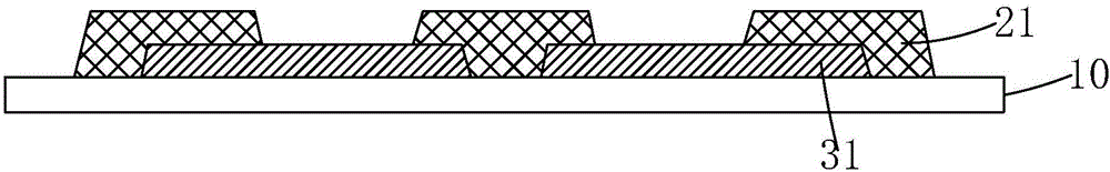
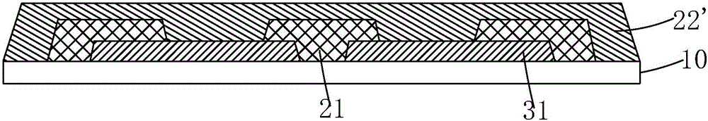
[0033] Step 1, such as figure 2 As shown, a TFT substrate 10 is provided, a layer of organic material is coated on the TFT substrate 10, and it is patterned through a yellow light process to form several organic material dams 21. The organic material The material dam 21 has side surfaces and an upper surface.

[0034] Specifically, the upper surface of the TFT substrate 10 provided in step 1 is provided with a first electrode 31 for constituting an OLED device, and the first electrode 31 is used as an anode or a cathode of the OLED device.

[0035] Specifically, in the step 1, the material of the...


PUM

PropertyMeasurementUnit
thicknessaaaaaaaaaa
thicknessaaaaaaaaaa

Abstract

The invention provides a manufacturing method for a pixel defining layer and a manufacturing method for an OLED device. According to the manufacturing method for the pixel defining layer, an inorganic covering layer is formed on side faces of organic material dam bodies to obtain multiple pixel isolation dams; then the multiple pixel isolation dams are subjected to plasma hydrophobic treatment to enable the upper surfaces of the organic material dam bodies to be hydrophobic in order to form the pixel defining layer; the upper surfaces of the pixel isolation dams are hydrophobic, so that ink can well enter pixel grooves without causing residue on the upper surfaces of the pixel isolation dams; the hydrophilic inorganic coating layer is arranged on the side faces of the pixel isolation dams, so that the ink can be well paved; a relatively large contact angle and a relatively thin film thickness are not caused by hydrophobicity of the side face; in addition, the side faces of the pixel isolation dams adopt the inorganic material; compared with the organic material, the inorganic material is more stable and higher in insulation; and meanwhile, the pixel defining layer is in contact with the OLED material, so that the OLED material can be more stable, and the service life of the OLED material can be prolonged.

Description

technical field [0001] The invention relates to the field of display technology, in particular to a method for manufacturing a pixel defining layer and a method for manufacturing an OLED device. Background technique [0002] Organic Light Emitting Diodes (OLED) displays have self-illumination, low driving voltage, high luminous efficiency, short response time, high definition and contrast, wide viewing angle, and wide operating temperature range. With many advantages such as color display, it is recognized by the industry as the display device with the most development potential. [0003] OLEDs have an anode, an organic functional layer, and a cathode sequentially formed on a substrate. At present, all functional material layers and cathode metal layer thin films of OLEDs are prepared by vacuum thermal evaporation process, that is, organic small molecule materials are heated in a vacuum cavity to sublimate or melt and gasify them into material vapors, which pass through a m...

Claims


Application Information

Patent Timeline
Patent Type & Authority Applications(China)
IPC IPC(8): H01L51/50H01L51/52H01L51/56
CPCH10K50/11H10K2101/40H10K50/80H10K71/00
Inventor 周星宇李松杉
Owner SHENZHEN CHINA STAR OPTOELECTRONICS TECH CO LTD
Why Eureka
Try Eureka