Electrochromic Device
An electrochromic, transparent conductive layer technology, applied in nonlinear optics, instrumentation, optics, etc., can solve the problems of undrawn, extra mold opening, and troublesome process, achieving overall sense and simple and beautiful design, saving mold opening Costs, hassle-free effect
- Summary
- Abstract
- Description
- Claims
- Application Information
AI Technical Summary
Problems solved by technology
Method used
Image
Examples
Embodiment Construction
[0022] The present invention will be described in detail below with reference to the drawings and embodiments. It should be noted that in the following description, similar elements are denoted by the same numbers.
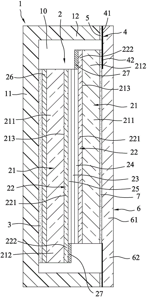
[0023] Refer to image 3 , The first embodiment of the electrochromic device of the present invention includes: an outer frame 1, an electrochromic element 2, a first adhesive layer 3, a modified frame layer 4, a second adhesive layer 5, and a transparent The protective plate 6, and an optical glue 7.
[0024] The outer frame 1 is made of, for example, plastic, and includes a frame body 11 located at the rear side of the electrochromic element 2 and substantially in the shape of an upright plate, and a frame winding body extending forward from the peripheral edge of the frame body 11 12. The frame surrounding body 12 and the frame body 11 jointly define a container 10 with an opening facing forward.
[0025] The electrochromic element 2 is disposed in the container 10 o...
PUM
| Property | Measurement | Unit |
|---|---|---|
| thickness | aaaaa | aaaaa |
Abstract
Description
Claims
Application Information
 - R&D
- Intellectual Property
- Life Sciences
- Materials
- Tech Scout
- Unparalleled Data Quality
- Higher Quality Content
- 60% Fewer Hallucinations
Browse by: Latest US Patents, China's latest patents, Technical Efficacy Thesaurus, Application Domain, Technology Topic, Popular Technical Reports.
© 2025 PatSnap. All rights reserved.Legal|Privacy policy|Modern Slavery Act Transparency Statement|Sitemap|About US| Contact US: help@patsnap.com


