Mask plate-based secondary exposure method for integrated circuit substrate

An integrated circuit-based, secondary exposure technology, applied in the semiconductor field, can solve the problems of affecting production, reducing the exposure efficiency of laser exposure machines, and consuming a lot of time, so as to achieve the effects of increasing production capacity, accelerating exposure efficiency, and simple operation

Active Publication Date: 2016-11-23
WUXI ZHONGWEI MASK ELECTRONICS
View PDF5 Cites 6 Cited by
  • Summary
  • Abstract
  • Description
  • Claims
  • Application Information

AI Technical Summary

Problems solved by technology

However, it will take about 10 to 15 minutes to perform alignment at each alignment mark, and it will take more than an hour to complete the alignment of the four points, while the exposure time of the basic board

Method used


Image

  • Mask plate-based secondary exposure method for integrated circuit substrate
  • Mask plate-based secondary exposure method for integrated circuit substrate
  • Mask plate-based secondary exposure method for integrated circuit substrate

Examples


Embodiment Construction

[0039] The present invention will be described in further detail below in conjunction with the accompanying drawings and specific embodiments. It should be noted that the specific details of the present invention described below are only for illustrating the present invention, and do not constitute a limitation to the present invention. Any modifications and variations made in accordance with the teachings of the invention as described are also within the scope of the invention.

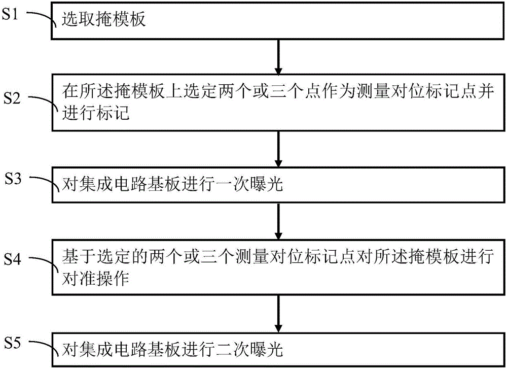
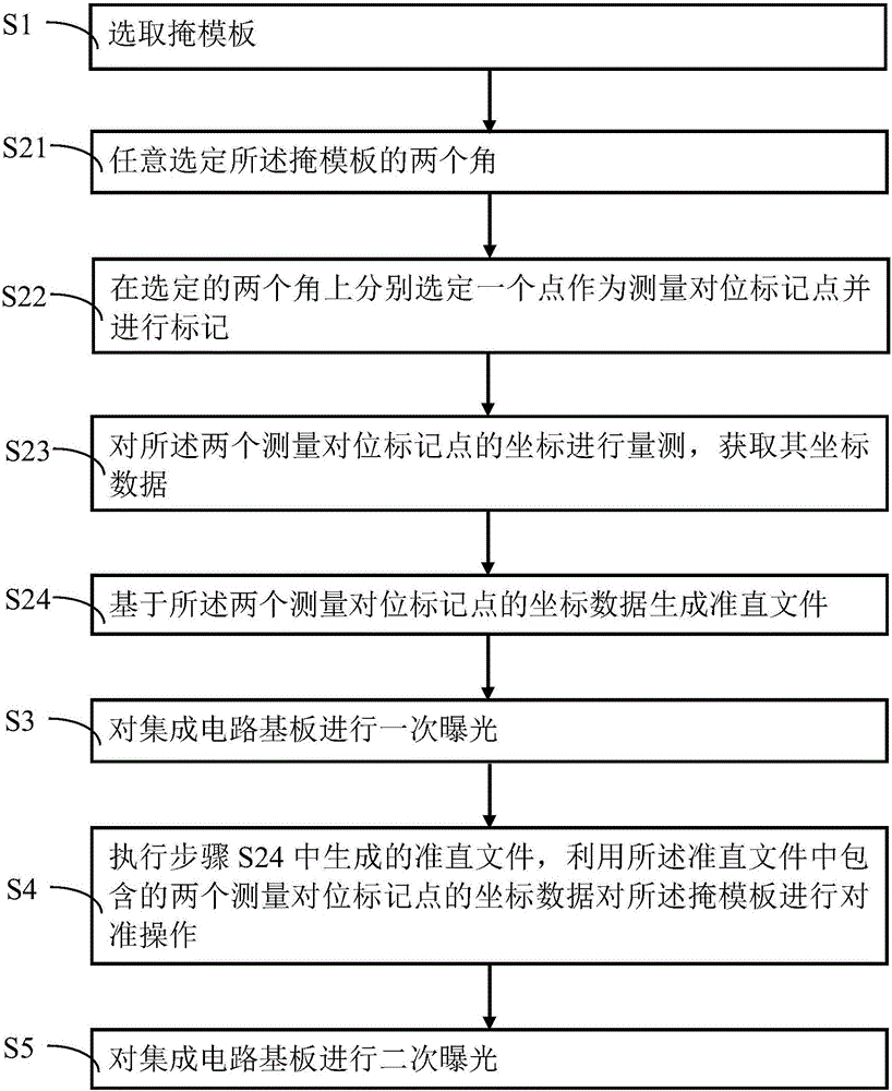
[0040] like figure 1 As shown, it is a schematic flow chart of an embodiment of a mask-based integrated circuit substrate secondary exposure method provided by the present invention. It can be seen from the figure that the integrated circuit substrate secondary exposure method includes: S1 Selecting a mask ; S2 selects two or three points on the mask as the measurement alignment mark points and marks them; S3 exposes the integrated circuit substrate once; S4 aligns the mask based on the selected two...


PUM


Abstract

The invention belongs to the technical field of semiconductors and discloses a mask plate-based secondary exposure method for an integrated circuit substrate. The method comprises the steps of S1, selecting a mask plate; S2, selecting two or three points on the mask plate to serve as measurement alignment mark points and performing marking; S3, performing primary exposure on the integrated circuit substrate; S4, performing alignment operation on the mask plate based on the selected two or three measurement alignment mark points; and S5, performing secondary exposure on the integrated circuit substrate. According to the method, the alignment operation is performed according to alignment based on obtained coordinate data after the integrated circuit substrate is subjected to the primary exposure, and then the integrated circuit substrate is subjected to the secondary exposure, so that the alignment operation time in the secondary exposure process is effectively shortened, the exposure efficiency is improved, and the production capacity is increased.

Description

technical field [0001] The invention belongs to the technical field of semiconductors, in particular to a secondary exposure method for an integrated circuit substrate. Background technique [0002] In the manufacturing process of semiconductors, integrated circuits, photovoltaic products and other electronic products, it is necessary to perform exposure treatment on various substrates represented by semiconductor wafers and photomasks. These substrates also include liquid crystal displays, glass substrates for plasma displays, magnetic disks, optical Disk motherboards, etc., are collectively referred to as masks below. A secondary exposure process is usually required for high-order masks (eg, advanced phase-shift mask lamps) or for necessary defect repairs. [0003] Before the second exposure process of the mask, since the images presented by the first exposure, development, etching and other processes already exist on the substrate, the position of the mask needs to be ca...

Claims


Application Information

Patent Timeline
IPC IPC(8): G03F7/20G03F9/00
CPCG03F7/70G03F9/7046
Inventor 沙云峰
Owner WUXI ZHONGWEI MASK ELECTRONICS
Why Eureka
Try Eureka