Method for forming 3D NAND flash memory

A technology of flash memory and step area, which is applied in the field of forming 3D NAND flash memory, can solve the problems of increased PR requirements, long process flow, and many process steps, and achieve the effect of saving process cost and reducing process steps

Active Publication Date: 2016-12-07
WUHAN XINXIN SEMICON MFG CO LTD
View PDF4 Cites 12 Cited by
  • Summary
  • Abstract
  • Description
  • Claims
  • Application Information

AI Technical Summary

Problems solved by technology

[0004] The current etching method is one PR mask (reticle) or trimming, one etching, and one step; resulting in many process steps, long process flow, increased requirements for PR, and s

Method used


Image

  • Method for forming 3D NAND flash memory
  • Method for forming 3D NAND flash memory
  • Method for forming 3D NAND flash memory

Examples


Embodiment Construction

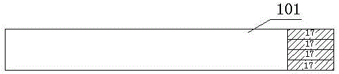
[0029] Such as figure 1 As shown, the present invention discloses a method for forming 3D NAND flash memory, comprising:

[0030] Step 1, providing a PAD including a T-layer stack structure, the PAD includes an array area, a first step area and a second step area, and the first step area and the second step area are respectively located on both sides of the array area, wherein T=2 n , and n≥2.

[0031] In a preferred embodiment of the present invention, each layer of the laminated structure includes silicon nitride and silicon oxide.

[0032] In a preferred embodiment of the present invention, the step of forming a PAD comprising a T-layer stack structure includes:

[0033] providing a substrate;

[0034] T sub-silicon nitride and silicon oxide are alternately deposited on the substrate to form a PAD with a stacked structure of T layers.

[0035] Step 2, use 1+㏒ 2 N-channel photomasks etch the PAD to form N steps in the first step area and the second step area, wherein t...


PUM


Abstract

The invention relates to the technical field of semiconductor manufacturing, in particular to a method for forming a 3D NAND flash memory. The method comprises the steps that firstly, different stairs are made on the part where steps are opened through 1+log2N levels of light covers and the etching technology to form differences; then, 2N stairs are etched at a time through 1 level of a light cover or PR trimming and etching. Thus, the technological steps are reduced, and meanwhile technological cost is reduced.

Description

technical field [0001] The invention relates to the technical field of semiconductor manufacturing, in particular to a method for forming 3D NAND flash memory. Background technique [0002] With the development of planar flash memory, the production process of semiconductors has made great progress. However, in recent years, the development of planar flash memory has encountered various challenges: physical limits and existing development technology limits. In this context, in order to solve the difficulties encountered in planar flash memory and to pursue lower production costs per unit storage unit, various three-dimensional flash memory structures have emerged as the times require. [0003] With the development of 3D technology, there are more and more film stacks, more and more steps (staircase), the number of step etching (etch) and the number of PR trimming (Trim) also increase accordingly , the requirements for the thickness and etching of PR also increase according...

Claims


Application Information

Patent Timeline
IPC IPC(8): H01L21/8247H01L27/115G11C16/02
CPCG11C16/02H10B69/00
Inventor 陈保友吴关平霍宗亮梅绍宁
Owner WUHAN XINXIN SEMICON MFG CO LTD
Why Eureka
Try Eureka