A production process of epitaxial wafers for power chips

A production process and power chip technology, applied in the field of epitaxial wafer production process for power chips, can solve the problems of poor thickness uniformity and resistivity uniformity of silicon epitaxial wafers, solid-state diffusion of substrate impurities, and uneven thermal field distribution, etc. Effects of good growth interface, elimination of solid state diffusion and natural doping phenomena, good thickness uniformity and resistivity uniformity

Active Publication Date: 2017-05-24
四川广瑞半导体有限公司
View PDF1 Cites 0 Cited by
  • Summary
  • Abstract
  • Description
  • Claims
  • Application Information

AI Technical Summary

Problems solved by technology

Nowadays, when preparing silicon epitaxial wafers, the thermal field distribution in the silicon wafer is not uniform, and there are solid-state diffusion and natural doping of substrate impurities, which lead to poor thickness uniformity and resistivity uniformity of the prepared silicon epitaxial wafers.
How to improve the existing silicon epitaxial wafer preparation process to improve the thickness uniformity and resistivity uniformity of silicon epitaxial wafers has become a problem that people generally pay attention to. However, there is no corresponding process and no related research. to report

Method used


Image

  • A production process of epitaxial wafers for power chips
  • A production process of epitaxial wafers for power chips
  • A production process of epitaxial wafers for power chips

Examples


Embodiment

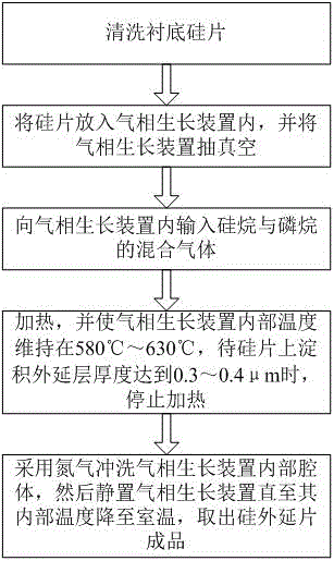
[0041] like figure 1 As shown, a production process of epitaxial wafers for power chips includes the following steps: step 1, cleaning the substrate silicon wafer; step 2, putting the cleaned silicon wafer into a vapor phase growth device, and vacuumizing the vapor phase growth device; Step 3, input the mixed gas of silane and phosphine into the vapor phase growth device; Step 4, heat, and keep the internal temperature of the vapor phase growth device at 580°C-630°C, until the thickness of the epitaxial layer deposited on the silicon wafer reaches 0.3-0.4 μm, stop heating; step 5, use nitrogen to flush the internal cavity of the vapor phase growth device to ensure that there is no reaction gas in the internal cavity of the vapor phase growth device, then let the vapor phase growth device stand until the internal temperature drops to room temperature, and take out the silicon epitaxial wafer finished product. In the specific implementation of this embodiment, the vacuum degree...


PUM


Abstract

The invention discloses an epitaxial wafer production process for a power chip. The epitaxial wafer production process includes the following steps that: step 1, a substrate silicon wafer is washed; step 2, the washed silicon wafer is arranged in a vapor phase growth device, and the vapor phase growth device is vacuumized; step 3, a mixed gas of silane and phosphorane is inputted into the vapor phase growth device; step 4, heating is carried out, temperature inside the vapor phase growth device is maintained at 580 DEG C to 630 DEG C, and heating is stopped when the thickness of a deposited epitaxial layer on the silicon wafer reaches 0.3 to 0.4 micron; and step 5, nitrogen is adopted to flush the inner cavity of the vapor phase growth device, and the vapor phase growth device is allowed to stand until the temperature inside the vapor phase growth device drops to room temperature, and a finished silicon epitaxial wafer is taken out. The epitaxial wafer production process of the invention has the advantages of simple overall process, convenient operation and low cost. With the epitaxial wafer production process adopted, the thickness uniformity and resistivity uniformity of the silicon epitaxial wafer can be improved.

Description

technical field [0001] The invention relates to a semiconductor material preparation technology, in particular to a production process of an epitaxial wafer for a power chip. Background technique [0002] At present, power chips are used more and more widely, and higher requirements are put forward for their performance. As an important part of the production process of epitaxial wafers for power chips, the performance of silicon epitaxial wafers has attracted more and more attention. Nowadays, when silicon epitaxial wafers are prepared, the thermal field distribution in the silicon wafers is not uniform, and there are substrate impurity solid-state diffusion and natural doping phenomena, which lead to poor thickness uniformity and resistivity uniformity of the prepared silicon epitaxial wafers. How to improve the existing silicon epitaxial wafer preparation process to improve the thickness uniformity and resistivity uniformity of silicon epitaxial wafers has become a proble...

Claims


Application Information

Patent Timeline
Patent Type & Authority Patents(China)
IPC IPC(8): H01L21/20H01L21/02
CPCH01L21/02H01L21/20
Inventor 王作义胡宝平陈小铎崔永明马洪文白磊
Owner 四川广瑞半导体有限公司
Why Eureka
Try Eureka