Method for Automatic Monitoring of Film Thickness Uniformity

A technology with uniform film thickness and automatic monitoring. It is used in instruments, semiconductor/solid-state device testing/measurement, measurement devices, etc., and can solve problems such as abnormal product quality.

Active Publication Date: 2018-11-23
POWERCHIP SEMICON MFG CORP
View PDF4 Cites 0 Cited by
  • Summary
  • Abstract
  • Description
  • Claims
  • Application Information

AI Technical Summary

Problems solved by technology

When the production process machine begins to age, and the film thickness data and film thickness distribution have slight changes, the above slight changes are likely to be the factors that cause abnormal product quality
However, the current existing technology is still unable to effectively and timely know the slight changes in the film thickness distribution

Method used


Image

  • Method for Automatic Monitoring of Film Thickness Uniformity
  • Method for Automatic Monitoring of Film Thickness Uniformity
  • Method for Automatic Monitoring of Film Thickness Uniformity

Examples


Embodiment Construction

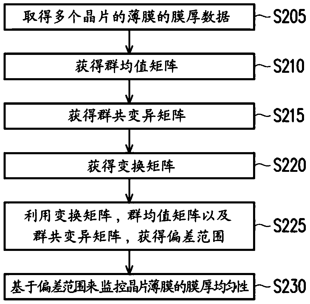
[0042] In the wafer manufacturing process, when the film thickness data and film thickness distribution change, the quality will also start to be abnormal at the same time. Therefore, in order to detect abnormalities early, the present invention proposes a method for automatically monitoring the uniformity of film thickness. The measured data are used to automatically carry out monitoring procedures. In order to make the content of the present invention clearer, the following specific examples are given as examples in which the present invention can actually be implemented.

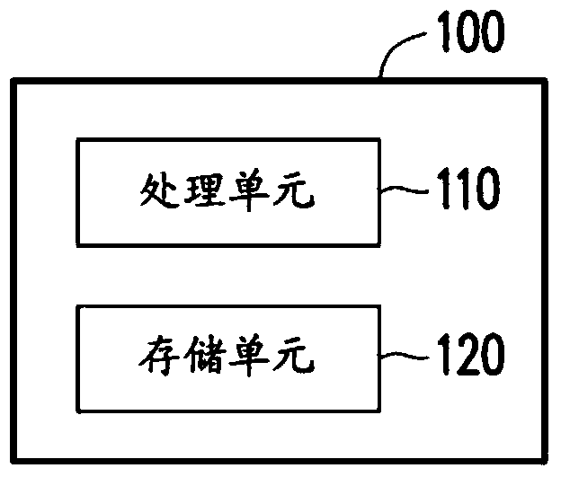
[0043] figure 1 is a block diagram of a monitoring device for film thickness uniformity according to an embodiment of the present invention. Please refer to figure 1 , the monitoring device 100 includes a processing unit 110 and a storage unit 120 . Here, the processing unit 110 is coupled to the storage unit 120 . The processing unit 110 is, for example, a central processing unit (Central Processing ...


PUM


Abstract

The invention provides a method for automatically monitoring film thickness uniformity. The method comprises the steps of acquiring the film thickness data of thin films of multiple wafers, wherein the film thickness data of each wafer comprises a plurality of thickness values in multiple measuring areas and the thickness values of each wafer are set as a film thickness vector; acquiring a cluster mean matrix based on the thickness values acquired from the measuring areas; acquiring a cluster synchronic variation matrix according to the cluster mean matrix and the film thickness vector; acquiring a transformation matrix according to the deviation relationships between the measuring areas; acquiring a deviation range by using the transformation matrix, the cluster mean matrix and the cluster synchronic variation matrix; monitoring the film thickness uniformity of the wafers based on the deviation range.

Description

technical field [0001] The invention relates to a semiconductor manufacturing technology, and in particular to a method for automatically monitoring the uniformity of film thickness. Background technique [0002] In the field of the semiconductor industry, a thin film is formed on the surface of the material by various methods in order to impart certain characteristics to the material used. The film thickness uniformity of the film formed by the film forming machine is directly related to the yield rate of the product and the quality of the film. When the production process machine begins to age, the film thickness data and film thickness distribution have slight changes, and the above slight changes are likely to be the factors that cause abnormal product quality. However, the current existing technology is still unable to effectively and timely know the slight changes in the film thickness distribution. Contents of the invention [0003] The purpose of the present inve...

Claims


Application Information

Patent Timeline
Patent Type & Authority Patents(China)
IPC IPC(8): H01L21/66G01B21/08
CPCG01B21/08G01B2210/56H01L22/12
Inventor 周明宽吕建辉曾筠捷施介文
Owner POWERCHIP SEMICON MFG CORP
Why Eureka
Try Eureka