Circuit board and manufacturing method thereof

A manufacturing method and circuit board technology, applied in the fields of printed circuit manufacturing, printed circuit, printed circuit, etc., can solve problems such as adverse effects of signal transmission, friction or bending of electroplated wires, poor bending resistance, etc., to achieve increased wiring space, Ensure the electrical quality and facilitate the design of thin lines

Active Publication Date: 2017-01-04
AVARY HLDG (SHENZHEN) CO LTD +2
View PDF3 Cites 6 Cited by
  • Summary
  • Abstract
  • Description
  • Claims
  • Application Information

AI Technical Summary

Problems solved by technology

[0002] Generally speaking, in order to perform surface treatment on the solder pad area exposed in the solder mask opening after the solder mask is formed, the solder pad will be connected to some lines extending outward to the edge area of ​​the board. For signal transmission, it is only used as an electrical connection pad to be able to plate metal on the pad, so it is generally called a plating wire. In the final product, the plating wire covered by the solder mask will not be removed and will remain in the solder mask. Layer, this part of the remaining plating wire will have an adverse effect on signal transmission
In addition, the electroplated wires in the gold finger area are thin and adjacent to the terminals. After repeated plugging and unplugging operations, the electroplated wires are prone to friction or bending with external mechanisms, and the flex resistance is poor.

Method used


Image

  • Circuit board and manufacturing method thereof
  • Circuit board and manufacturing method thereof
  • Circuit board and manufacturing method thereof

Examples


Embodiment Construction

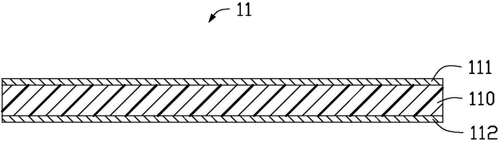
[0042] An embodiment of the present invention provides a method for manufacturing a circuit board 10, comprising steps:

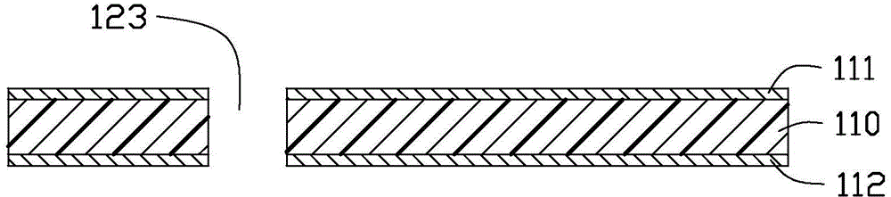
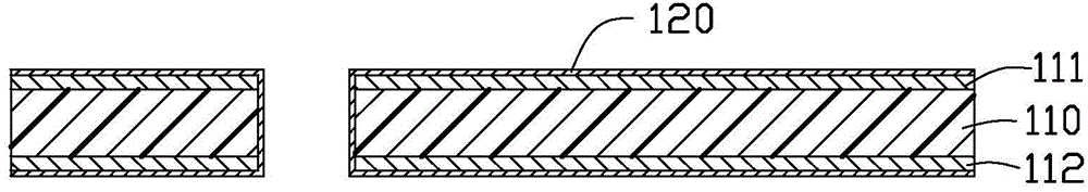
[0043] For a first step, see figure 1 , providing a substrate 11 comprising a base layer 110 and a continuous first copper foil layer 111 and a continuous second copper foil layer 112 formed on two opposite surfaces of the base layer 110 .

[0044] In this embodiment, the base layer 110 is a flexible resin layer, such as polyimide (Polyimide, PI), polyethylene terephthalate (Polyethylene Terephthalate, PET) or polyethylene naphthalate (Polythylene Naphthalate, PEN); In other embodiments, the base layer 110 may also be a multi-layer flexible substrate, including multiple resin layers and multiple conductive circuit layers arranged alternately. The thickness of the first copper foil layer 111 and the second copper foil layer 112 is uniform. In this embodiment, the thickness of the first copper foil layer 111 and the second copper foil layer 112 is the same. ...


PUM


Abstract

The invention provides a manufacturing method of a circuit board. The method comprises the steps that a substrate is provided, wherein the substrate comprises a substrate layer and a continuous first copper foil layer formed at one side of the substrate layer; a conductive layer is formed through electroplating in one part of area of the first copper foil layer; a surface treatment pattern is formed through electroplating on one part of surface of the conductive layer; the first copper foil layer which is not covered by the conductive layer is etched and removed, and meanwhile, the conductive layer which is not covered by the surface treatment pattern is thinned; and the left first copper foil layer on the surface of the substrate layer and the conductive layer become conductive line patterns to obtain the circuit board free of an electroplating wire. The invention further relates to the circuit board, obtained by the manufacturing method, free of the electroplating wire.

Description

technical field [0001] The invention relates to a circuit board and a manufacturing method thereof. Background technique [0002] Generally speaking, in order to perform surface treatment on the solder pad area exposed in the solder mask opening after the solder mask is formed, the solder pad will be connected to some lines extending outward to the edge area of ​​the board. For signal transmission, it is only used as an electrical connection pad to be able to plate metal on the pad, so it is generally called a plating wire. In the final product, the plating wire covered by the solder mask will not be removed and will remain in the solder mask. Layer, this part of the remaining plating wire will have an adverse effect on signal transmission. In addition, the electroplated wires in the gold finger area are thinner and adjacent to the terminals. After repeated plugging and unplugging operations, the electroplated wires are prone to friction or bending with external mechanisms,...

Claims


Application Information

Patent Timeline
IPC IPC(8): H05K3/06H05K3/28
CPCH05K3/06H05K3/282H05K2203/0353H05K3/108H05K3/244H05K3/427H05K2201/0154H05K2201/0338H05K2201/09736H05K2201/098H05K2203/0723H05K2203/1394
Inventor 苏威硕
Owner AVARY HLDG (SHENZHEN) CO LTD
Why Eureka
Try Eureka