Organic tribotronics transistor and contact electrification gate-controlled light-emitting device

A technology of transistors and electronics, applied in the field of optoelectronics, to achieve the effect of wide selection of semiconductor materials, good control characteristics, and low cost

Active Publication Date: 2017-01-18
BEIJING INST OF NANOENERGY & NANOSYST
View PDF4 Cites 5 Cited by
  • Summary
  • Abstract
  • Description
  • Claims
  • Application Information

AI Technical Summary

Problems solved by technology

[0006] In view of the above technical problems, the present invention provides an organic triboelectronics transistor and a contact electrification gated power generation device combining a triboelectric nanogen...

Method used


Image

  • Organic tribotronics transistor and contact electrification gate-controlled light-emitting device
  • Organic tribotronics transistor and contact electrification gate-controlled light-emitting device
  • Organic tribotronics transistor and contact electrification gate-controlled light-emitting device

Examples


Embodiment Construction

[0036] The invention uses organic materials to develop triboelectronic devices, and combines them with organic light-emitting devices to realize a new way of regulating device light emission by mechanical input, and to display human-computer interaction devices that regulate electroluminescent functions by external forces.

[0037] In order to make the purpose, technical solutions and advantages of the present invention more clear, the present invention will be further described in detail below in conjunction with specific implementation methods and with reference to the accompanying drawings.

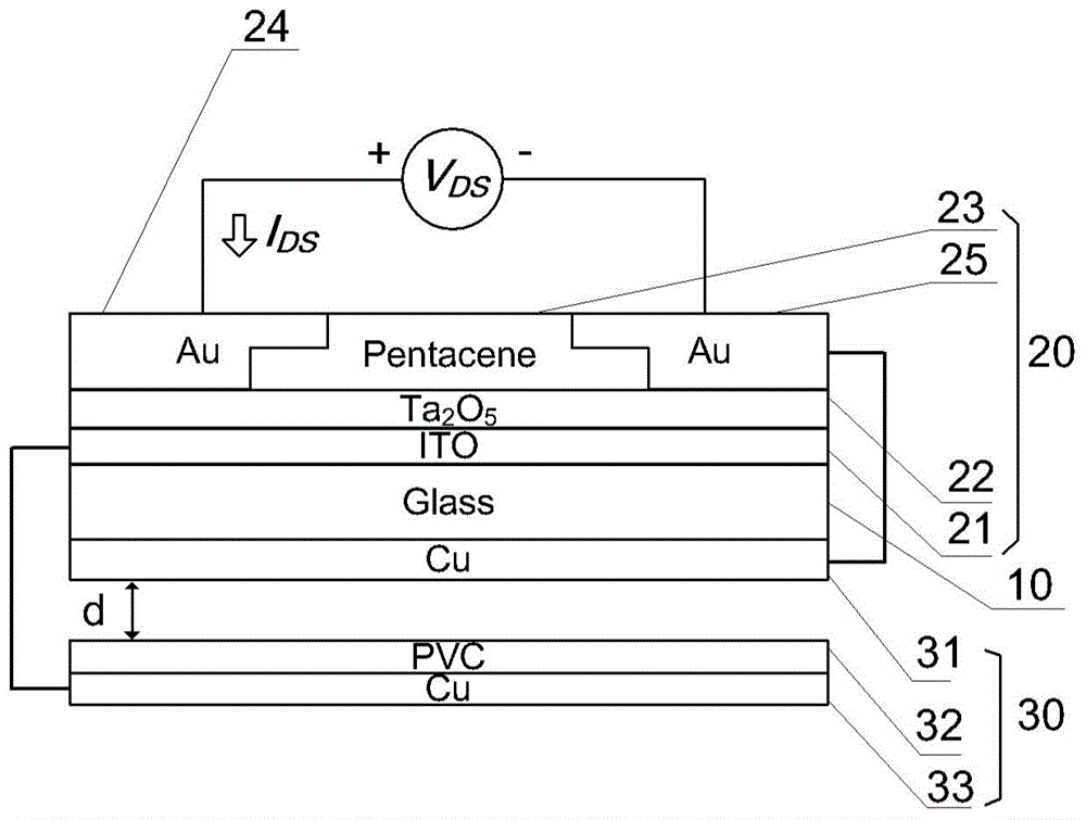
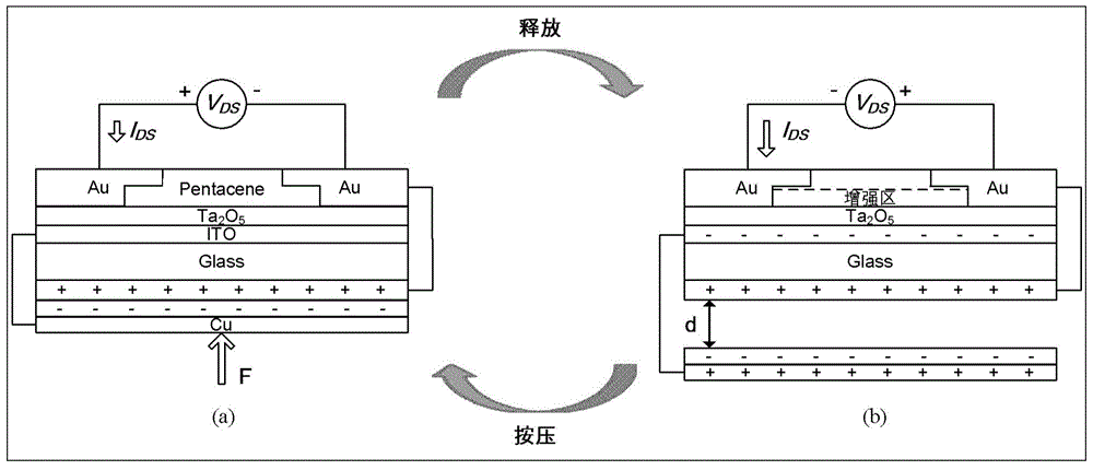
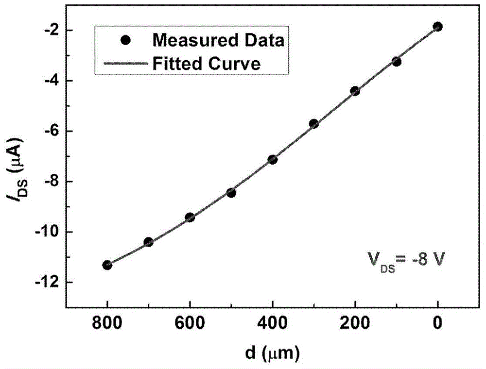
[0038] In a first exemplary embodiment of the present invention, an organic triboelectronic transistor is provided. figure 1 It is a schematic structural diagram of an organic triboelectronics transistor according to an embodiment of the present invention. Such as figure 1 As shown, the organic triboelectronic transistor of this embodiment is based on an organic thin film transistor s...


PUM


Abstract

The invention provides an organic tribotronics transistor. The organic tribotronics transistor comprises a substrate, an organic thin-film transistor formed above the substrate and a frictional nano generator formed below the substrate. The frictional nano generator comprises a static friction portion formed at the lower surface of the substrate and a movable friction portion arranged opposite to the static friction portion, wherein one of the static friction portion and the movable friction portion is electrically connected with a source electrode of the organic thin-film transistor, and the other is electrically connected with a grid electrode of the organic thin-film transistor. The organic tribotronics transistor utilizes electrostatic potential generated by a frictional generator to act as a gate electrode gate signal so as to realize regulation and control for transport characteristics of carriers in a semiconductor, thereby having good regulation and control characteristics, and realizing a brand new mode of regulating and controlling light emission of a device through mechanical input. Based on the organic tribotronics transistor, the invention further provides a contact electrification gate-controlled light-emitting device.

Description

technical field [0001] The invention relates to the technical field of optoelectronics, in particular to an organic triboelectronics transistor and a contact electrification gate-controlled light-emitting device. Background technique [0002] Organic light-emitting transistor is a new type of organic optoelectronic device, which integrates the switching function of organic field-effect transistor and the light-emitting function of organic light-emitting diode, and can regulate the luminous intensity of the device through the gate voltage. And the field of lasers shows potential application prospects. Although the technology of organic light-emitting transistors is very mature, in view of the three-terminal structure of the device unit, it is necessary to provide a special gate power supply and realize regulation through electrical signals, and there is no mechanism for direct interaction between the external environment and the light-emitting device. [0003] Combining the ...

Claims


Application Information

Patent Timeline
IPC IPC(8): H01L51/42H01L51/50
CPCH10K30/00H10K50/00Y02E10/549
Inventor 张弛王中林韩昌报张丽敏
Owner BEIJING INST OF NANOENERGY & NANOSYST
Why Eureka
Try Eureka