Eureka AIR delivers breakthrough ideas for toughest innovation challenges, trusted by R&D personnel around the world.

Robust high performance semiconductor package

A semiconductor and substrate technology, applied in the field of robust and high-performance semiconductor packaging, can solve problems such as damage to power semiconductor devices and thermal stress of circuit devices

Active Publication Date: 2017-02-01
INFINEON TECH AMERICAS CORP
View PDF9 Cites 0 Cited by
  • Summary
  • Abstract
  • Description
  • Claims
  • Application Information

AI Technical Summary

Problems solved by technology

Also, due to the mismatch in the coefficient of thermal expansion (CTE) between the substrate and packaging materials, the substrate and package are subject to volumetric expansion and contraction at different rates, thereby introducing thermal stress that can damage power semiconductor devices and circuitry on the substrate

Method used


Image

  • Robust high performance semiconductor package
  • Robust high performance semiconductor package
  • Robust high performance semiconductor package

Examples


Embodiment Construction

[0013] The following description contains specific information pertaining to embodiments of the disclosure. The drawings in this application and their accompanying detailed description are directed at exemplary embodiments only. Unless stated otherwise, similar or corresponding elements among the figures may be indicated by similar or corresponding reference numerals. Furthermore, the drawings and illustrations in this application are generally not to scale and are not intended to correspond to actual relative dimensions.

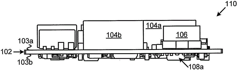
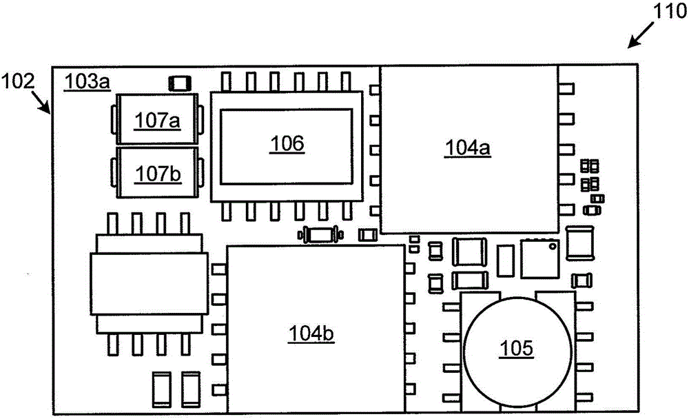
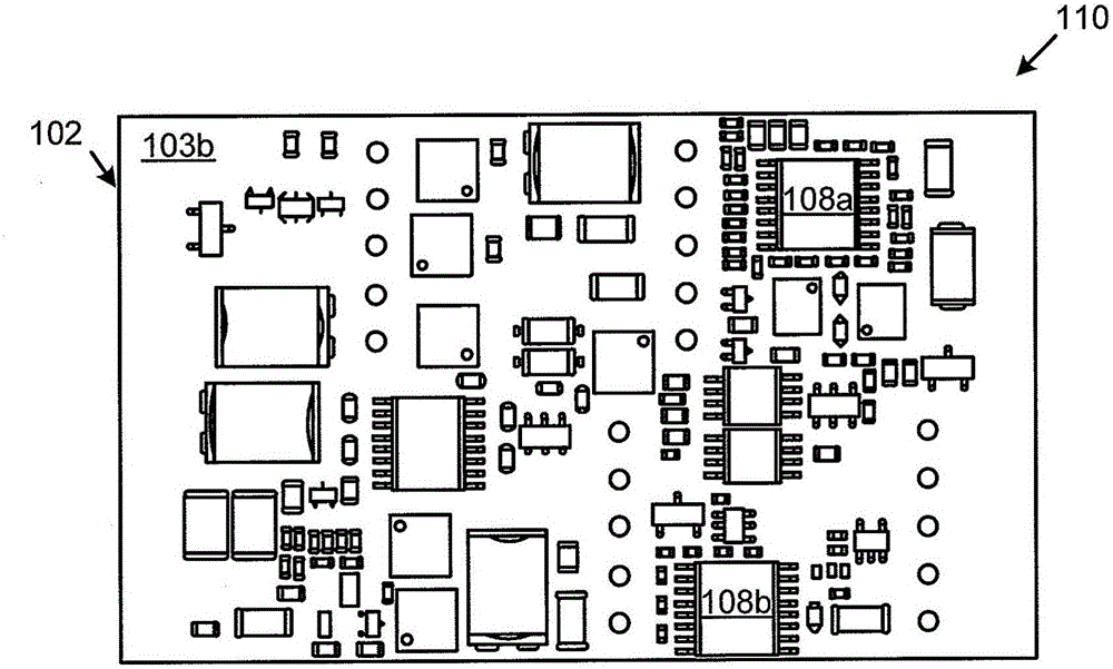
[0014] Figure 1A A side view of a substrate assembly according to one embodiment of the application is illustrated. Such as Figure 1A As shown, the substrate assembly 110 includes a substrate 102 and various electrical components and semiconductor devices integrated on the substrate 102 . For example, if Figure 1A-Figure 1C On top surface 103 a of substrate 102 are shown transformers 104 a and 104 b , ring inductor 105 , tantalum capacitor 106 , ceram...


PUM


Abstract

The application relates to robust high performance semiconductor package. The semiconductor package includes a suspended substrate having one or more semiconductor devices thereon, a metallic case covering the suspended substrate, the suspended substrate being supported by a plurality of mechanical leads on opposing sides of the semiconductor package, at least one of the plurality of mechanical leads having a coefficient of thermal expansion (CTE) that substantially matches a CTE of the suspended substrate, where at least one of the plurality of mechanical leads is electrically connected to the suspended substrate, and where the plurality of mechanical leads absorb mechanical shocks so as to prevent damage to the semiconductor package. The semiconductor package also includes a thermal gel between the suspended substrate and the metallic case. The suspended substrate can be a printed circuit board. The metallic case includes mounting ears for transferring heat away from the semiconductor package.

Description

[0001] This application claims the benefit of and priority to Provisional Patent Application Serial No. 62 / 196,799, filed July 24, 2015, entitled "Robust HighPerformance Semiconductor Package." The disclosure in this provisional application is hereby incorporated by reference in its entirety into this application. technical field [0002] The present application relates to semiconductor packaging, and more particularly to robust high performance semiconductor packaging. Background technique [0003] Semiconductor power modules control electrical power to circuits and devices such as motors, actuators, controllers, and the like. When high reliability is required for use in extreme or harsh environments, such as in high performance vehicles, aircraft, space shuttles and satellites, it is important to provide mechanically robust and thermally efficient semiconductor packages. For example, in some space and satellite applications, semiconductor packages with power semiconductor...

Claims


Application Information

Patent Timeline
Patent Type & Authority Applications(China)
IPC IPC(8): H01L25/07H01L23/373
CPCH01L23/373H01L25/072H01L23/42H05K1/0216H05K1/117H05K2201/10295H05K2201/1034H05K2201/10371H05K2201/10424H01L23/3675H01L25/18H01L23/057H01L23/24H01L23/562H01L23/49838H01L25/0655H01L25/162H01L24/00
Inventor W·帕廷顿
Owner INFINEON TECH AMERICAS CORP
Why Eureka
Eureka Blog
Learn More