A kind of nano-semiconductor photorefractive film material and preparation method thereof

A nano-semiconductor and thin-film material technology, which is applied in metal material coating process, vacuum evaporation plating, coating, etc., can solve the problems of complex process, material consumption, slow crystal growth cycle, etc., and achieve simple and easy preparation process, preparation The method is simple and easy, and the effect of easy industrial production

Inactive Publication Date: 2018-10-26
SHANDONG NORMAL UNIV
View PDF3 Cites 0 Cited by
  • Summary
  • Abstract
  • Description
  • Claims
  • Application Information

AI Technical Summary

Problems solved by technology

[0004] However, the existing photorefractive materials have the following disadvantages: 1. The crystal growth period is slow, the process is complicated, the application size is large, the processing is troublesome, and the material consumption is large; 2. An external electric field is required to redistribute the photogenerated carriers, so that The refractive index changes

Method used


Image

  • A kind of nano-semiconductor photorefractive film material and preparation method thereof
  • A kind of nano-semiconductor photorefractive film material and preparation method thereof
  • A kind of nano-semiconductor photorefractive film material and preparation method thereof

Examples


Embodiment 1

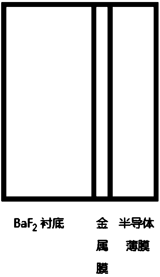
[0047] Wash BaF with absolute ethanol 2 Substrate, using 99.99% copper target, the sputtering chamber is evacuated to 5×10 -4 Pa, filled with argon, the working pressure of the sputtering chamber is 0.45Pa, the sputtering voltage is 300V, the current is 80mA, the sputtering rate is 0.08nm / s, and the sputtering time is 125s. 2 A transparent copper film of about 10nm is prepared on the substrate.

[0048] Using 99.99% PbTe target material, the sputtering chamber is evacuated to 5×10 -4Pa, filled with argon, the working pressure of the sputtering chamber is 0.45Pa, the sputtering power is 20W, the sputtering rate is 0.09nm / s, and the sputtering time is 1100s, so that a PbTe film of about 100nm is prepared on the transparent copper film, that is, BaF 2 / Cu / PbTe film.

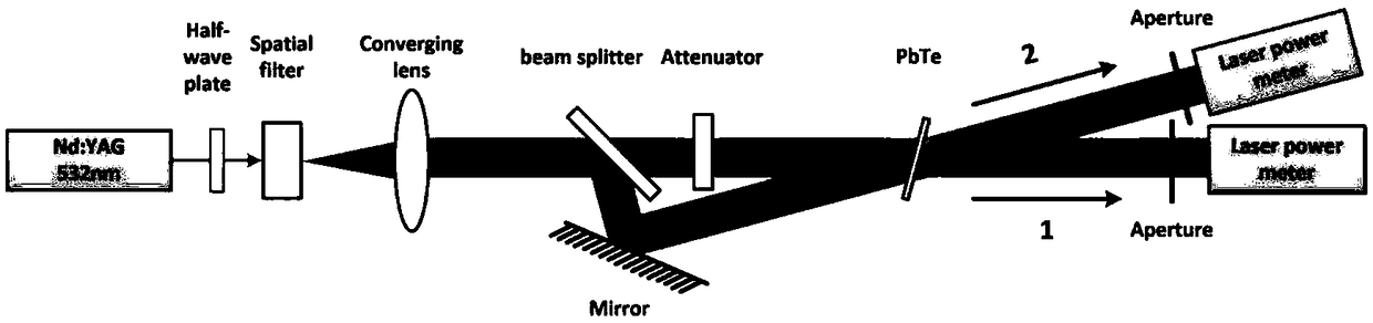
[0049] The prepared material structure is as figure 1 shown. BaF prepared by two-wave coupling experiments 2 / Cu / PbTe film for photorefractive effect test, such as figure 2 As shown, the two-wave coupling ex...

Embodiment 2

[0057] Wash BaF with absolute ethanol 2 The substrate is made of 99.99% PbTe target material, and the sputtering chamber is evacuated to 5×10 -4 Pa, filled with argon, sputtering chamber working pressure 0.45Pa, sputtering power 20W, sputtering rate 0.09nm / s, sputtering time 1100s, thus in BaF 2 A PbTe film of about 100nm is prepared on the substrate, that is, BaF 2 / PbTe film.

[0058] BaF prepared by two-wave coupling experiment 2 / PbTe film for photorefractive effect test, BaF 2 / PbTe film has weak photorefractive effect. The weaker photorefractive effect means that the diffraction efficiency of the grating obtained by taking pictures with a CCD (charge-coupled device) is very low, less than 0.1%, and the refractive index grating stripes read from the optical path diagram of the two-wave coupling experiment are very weak. BaF prepared in this embodiment 2 / PbTe thin film grating diffraction efficiency is very low, only 0.05%.

Embodiment 3

[0060] Wash BaF with absolute ethanol 2 Substrate, using 99.99% gold target, the sputtering chamber is evacuated to 5×10 -4 Pa, filled with argon, the working pressure of the sputtering chamber is 0.45Pa, the sputtering voltage is 340V, the current is 80mA, the sputtering rate is 0.19nm / s, and the sputtering time is 60s. 2 A transparent gold film of about 10nm was prepared on the substrate.

[0061] Using 99.99% PbTe target material, the sputtering chamber is evacuated to 5×10 -4 Pa, filled with argon, the working pressure of the sputtering chamber is 0.45Pa, the sputtering power is 20W, the sputtering rate is 0.09nm / s, and the sputtering time is 1000s, so that a PbTe film of about 100nm is prepared on the transparent silver film, that is, BaF 2 / Au / PbTe film.


PUM

PropertyMeasurementUnit
thicknessaaaaaaaaaa
thicknessaaaaaaaaaa
transmittivityaaaaaaaaaa

Abstract

The invention discloses a nano semiconductor photorefractive thin film material and a preparation method thereof. The nano semiconductor photorefractive thin film material comprises a metal thin film and a lead chalcogenide compound thin film, wherein one surface of the metal thin film is in contact with one surface of the lead chalcogenide compound thin film; and the work function of a metal of the metal thin film is greater than or equal to the electron affinity of a lead chalcogenide compound thin film semiconductor, or a schottky junction is formed on the contact interface of the metal thin film and the lead chalcogenide compound thin film. The preparation method comprises the steps of growing a layer of transparent metal thin film on a substrate, and then growing a layer of a lead chalcogenide compound thin film semiconductor material on the metal thin film. By the connection of the metal thin film to the lead chalcogenide compound thin film and the formation of the schottky junction on the interface of the metal thin film and the lead chalcogenide compound thin film, a built-in electric field is formed in the thin films, so that movement and redistribution of photon-generated carriers can be realized without an external electric field, and the aim of application of a photorefractive material is completely fulfilled.

Description

technical field [0001] The invention relates to a nano-semiconductor photorefractive film material and a preparation method thereof. Background technique [0002] The photorefractive effect refers to a special light-induced refractive index change phenomenon. The incident light excites the carriers (electrons or holes) trapped in the shallow wells formed by impurities or defects in certain crystals or organics. If the light intensity is uneven, the photoexcited carriers will pass through diffusion, etc. The process migrates, resulting in the appearance of a light-induced electric field in the medium. The light-induced electric field then produces a change in the refractive index through the electro-optic effect of the medium. However, the change of refractive index does not happen immediately, but requires a certain time to build up; even weak light, as long as the irradiation time is long enough, it can produce obvious photorefractive effect; only in the light field with ...

Claims


Application Information

Patent Timeline
Patent Type & Authority Patents(China)
IPC IPC(8): C23C14/18C23C14/06
CPCC23C14/0623C23C14/18
Inventor 曹文田
Owner SHANDONG NORMAL UNIV
Why Eureka
Try Eureka