IC (integrated circuit) testing device and method

A test device and a technology to be tested are applied in the direction of measuring devices, electronic circuit tests, and electrical measurements. It can solve the problems of tight IO pins of controllers, increased costs, and insufficient controllers, so as to reduce costs, simplify structures, and The effect of saving resources

Active Publication Date: 2017-02-22
HANGZHOU VANGO TECH
View PDF5 Cites 17 Cited by
  • Summary
  • Abstract
  • Description
  • Claims
  • Application Information

AI Technical Summary

Problems solved by technology

[0003] 1) When there are many IO pins of the chip to be tested, the IO pins of the controller may not be enough, so it is possible to use multiple controllers to test the chip to be tested. It is an increase in cost. The controllers here are generally FPGA chips, single-chip microcomputers (more powerful), DSP chips or ARM chips, etc. These chips are generally more expensive, and the design of printed circuit boards may be more complicated. , leading to an increase in the cost and difficulty of PCB design; in addition, the use of multiple controllers will increase the difficulty of development, debugging and maintenance
[0004] 2) At present, the number of IO pins of most chips to be tested is increasing, and each IO pin may be a combination of multiple functions. To test all the functions of a certain IO of the chip to be tested, multiple controll

Method used


Image

  • IC (integrated circuit) testing device and method
  • IC (integrated circuit) testing device and method
  • IC (integrated circuit) testing device and method

Examples


Embodiment 1

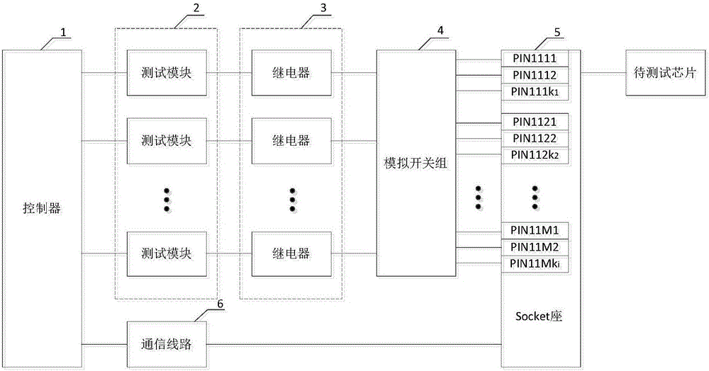
[0048] Please refer to figure 1 , figure 1 A schematic structural view of an IC testing device provided by the present invention, the testing device includes:

[0049] controller 1;

[0050] Specifically, the controller 1 here is used to control the peripheral modules in the IC testing device to complete the testing of the chip to be tested.

[0051] Socket 5 connected with the chip to be tested and used to connect the chip to be tested with the test device;

[0052] Socket 5 is used to connect the chip to be tested and the test device, so as to connect all the resources of the chip to be tested to the test device. For different packages and different types of chips to be tested, the connection between the chip to be tested and the test device can be completed by replacing different Socket seats 5. In addition, an adapter board can also be added to complete the connection between different chips to be tested and the test device. Connection.

[0053] N test modules 2 are u...

Embodiment 2

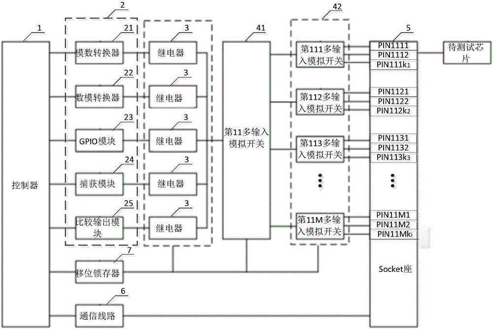
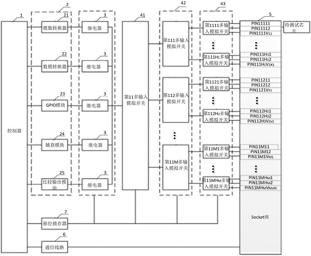
[0061] Please refer to figure 2 and image 3 ,in, figure 2 and image 3 All are structural schematic diagrams of another IC testing device provided by the present invention; on the basis of the IC testing device provided in Embodiment 1:

[0062] As preferably, the testing device also includes:

[0063] One end is connected to the controller 1, and the other end is respectively connected to the control end of the analog switch group 4 and the control ends of N relays 3. The shift latch 7 is used to receive the serial input of the controller 1. control the control terminal of the analog switch group 4 and the control signals of the N relays 3, and output the control signals to the analog switch group 4 and the relays 3 in parallel correspondingly when the chip to be tested is tested.

[0064] It can be understood that, in order to further save the IO resources of the controller 1, the IC testing device provided by the present application also includes a shift latch 7, and...


PUM


Abstract

The invention discloses an IC (integrated circuit) testing device and method. The device comprises a controller, a socket, N testing modules, N relays, an analog switch group and a communication circuit, a second end of the analog switch group is connected with the socket, a control end of the analog switch group is connected with the controller, L-level multi-input analog switches are cascaded to form the analog switch group, the analog switch group is used for selecting corresponding pins of a chip to be tested to connect with corresponding testing modules according to control of the controller, a first end of the communication circuit is connected with the controller, the other end of the communication circuit is connected with the socket, and the communication circuit is used for establishing communication between the controller and the socket. According to the testing device, the analog switch group formed by cascade of the L-level multi-input analog switches is arranged between the N testing modules and the socket for placing chips to be tested, pins of the chips to be tested cannot be directly with the controller when the chips to be tested are tested, a plurality of controller are omitted, controller resources are greatly saved, cost of the testing device is reduced, and structures of the testing device are simplified.

Description

technical field [0001] The invention relates to the technical field of chip testing, in particular to an IC testing device and method. Background technique [0002] With the development of microelectronics technology and the continuous increase of market demand for integrated chips, IC testing devices have also followed the continuous development. At present, the integration level of integrated chips is getting higher and higher, the functions are more and more complex, the performance requirements are getting higher and higher, and the power consumption requirements are getting lower and lower, but at the same time, the lower the cost, the better. At present, the number of pins of packaged integrated chips is increasing, up to hundreds or even thousands of pins, and each pin packaged may be multiplexed with multiple functions, and sold to customers in the integrated chip In the past, integrated chip manufacturers had to perform FT tests on each integrated chip to pick out ...

Claims


Application Information

Patent Timeline
IPC IPC(8): G01R31/28
CPCG01R31/2889
Inventor 卢杰
Owner HANGZHOU VANGO TECH
Why Eureka
Try Eureka