
A method for manufacturing a multi-layer large-size high-speed backplane with a size of 500mm*800mm or more

A high-speed backplane and manufacturing method technology, which is applied in multilayer circuit manufacturing, printed circuit manufacturing, printed circuit components, etc., can solve the problems of uneven back drilling methods, excessive depth, and insufficient pressing temperature of intermediate products, etc. , to achieve the effect of reducing investment in production equipment, reducing the number of layers and height, and ensuring the quality of lamination

Active Publication Date: 2019-05-17
HUIZHOU KING BROTHER CIRCUIT TECH +2
View PDF5 Cites 0 Cited by
  • Summary
  • Abstract
  • Description
  • Claims
  • Application Information

AI Technical Summary

Problems solved by technology

[0004] (1) The size of the product is very large, the number of layers is high, and the demand for plates is large. If one-time pressing is used, if one of the core plates is offset, it will lead to overall scrapping. For example: 48 layers, 23 core plates are used for production, and the material cost is high. , Excessive deviation of one core board during the lamination process will cause the remaining 22 core boards to be scrapped, and the cost loss will be serious, causing existing circuit board processing manufacturers to dare not accept this type of product;
[0005] (2) The number of product layers is high and the thickness is high. The total thickness of the product after lamination using 0.1mm core board + 0.05mm106 prepreg is >4mm. product scrapping;
[0006] (3) The size of large-scale high-speed printed circuit boards is large, generally above 500mm×800mm, and the maximum size of conventional drilling and forming machines is about 500mm×600mm, which cannot meet the requirements, resulting in the need to purchase large-size processing equipment or send out Substituting processing for other processors, it takes time to transport back and forth, and it is difficult to control the quality of outbound processing
Existing PCB factories have uneven back drilling methods, which are prone to problems of insufficient depth and excessive depth leading to scrapping, and are not suitable for the processing of large-size, high-layer, high-speed printed circuit boards

Method used


Image

  • A method for manufacturing a multi-layer large-size high-speed backplane with a size of 500mm*800mm or more
  • A method for manufacturing a multi-layer large-size high-speed backplane with a size of 500mm*800mm or more
  • A method for manufacturing a multi-layer large-size high-speed backplane with a size of 500mm*800mm or more

Examples


Embodiment Construction

[0059] In order to enable those skilled in the art to better understand the technical solution of the present invention, the product of the present invention will be further described in detail below in conjunction with the embodiments and accompanying drawings.

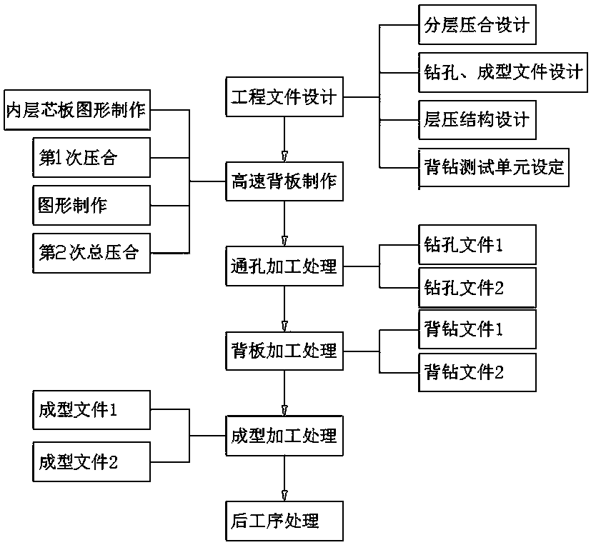
[0060] Such as Figure 1 to Figure 12 As shown, a method for manufacturing a multi-layer large-size high-speed backplane with a size of 500mm*800mm or more is characterized in that it includes the following steps:

[0061] The first step is engineering document design, including

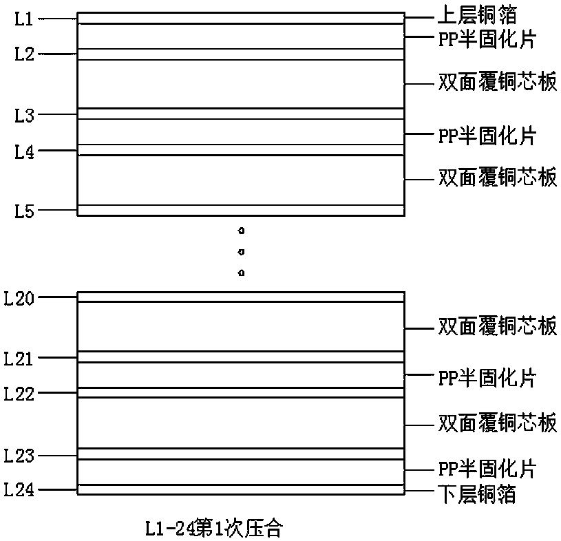
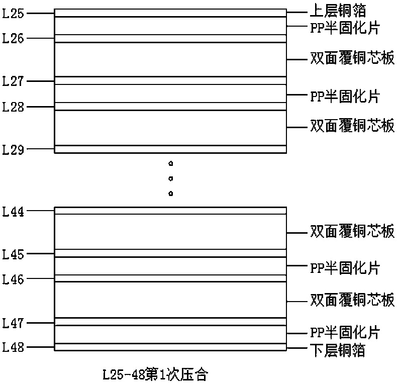
[0062] 1.1) Layered pressing design, the layered pressing is to change the conventional one-time pressing forming method into multiple pressing forming methods according to the number of layers of the product, specifically, the layered pressing is based on the number of product layers According to the number of layers, the products are divided into multiple groups, and the products of each group are pressed separately, and then the product...


PUM


Abstract

The invention discloses a fabrication method of a multilayer, large-size and high-speed back panel. The fabrication method comprises the following steps of (1), project file design, wherein the project file design comprises layered lamination design, drilling, formation file design, lamination structure design and setting of a back drilling test unit; (2), fabrication of the high-speed back panel, wherein the fabrication of the multilayer, large-size and high-speed back panel is performed according to the project file design; (3), through hole processing; (4), back drilling processing, in which fragmental back drilling processing is performed on the high-speed back panel according to a fragmental drilling file and the back drilling test unit in the step (1); (5) forming and processing, and processing is performed on the high-speed back panel according to the fragmental formation file in the step (1); and 6, post-procedure processing, in which package and shipment are performed after electrical detection and final inspection are performed according to a conventional circuit board processing flow. The fabrication method of the multilayer, large-size and the high-speed back panel has the advantages of good lamination quality, low rejection rate, low cost, rapid detection, high efficiency and the like.

Description

technical field [0001] The invention relates to the technical field of high-speed backplane production, in particular to a method for fabricating a multi-layer large-size high-speed backplane with a size of 500mm*800mm or more. Background technique [0002] The 10G and 15G technological changes in the information industry have put forward higher requirements for high-speed signal transmission and integrity, requiring high etching precision and strict impedance control. Communication base stations and large-scale industrial control equipment put forward the demand for multi-layer large-size high-speed backplanes. The products have high technical content and high added value. Many PCB manufacturers want to win market orders for this type of products. However, this type of high-speed backplane is easy to process The following problem occurs: [0003] 1. There are deficiencies in the production method of high-multilayer and large-size high-speed printed circuit boards: [0004...

Claims


Application Information

Patent Timeline
Patent Type & Authority Patents(China)
IPC IPC(8): H05K1/02H05K3/00H05K3/46
CPCH05K1/0268H05K3/0005H05K3/0047H05K3/4611H05K2203/162
Inventor 林启恒武守坤李敬虹李享唐宏华
Owner HUIZHOU KING BROTHER CIRCUIT TECH
Learn More