

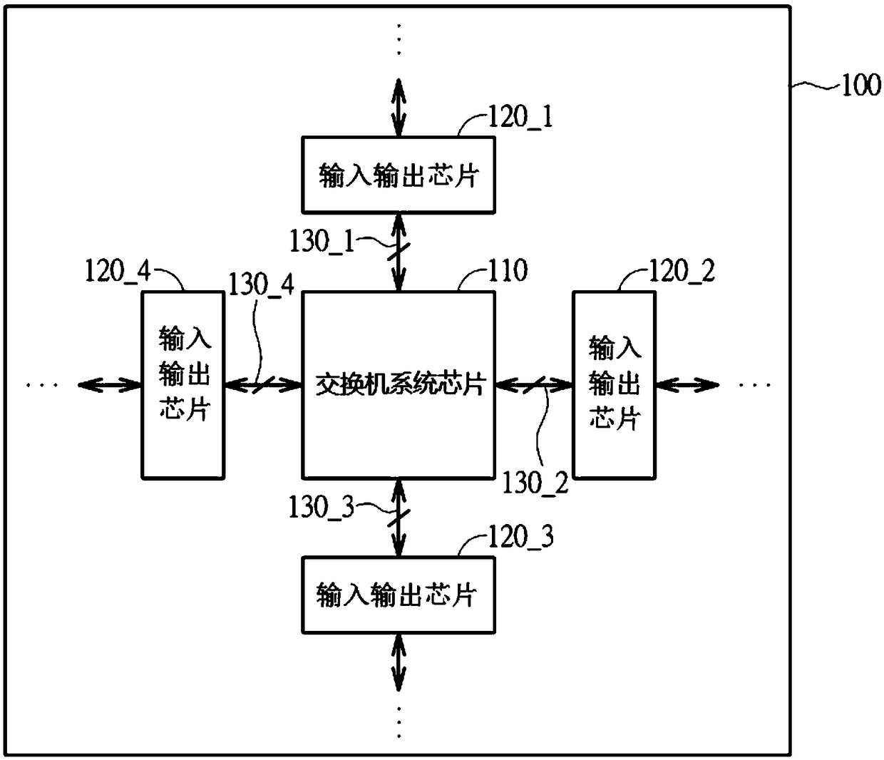
multi-chip structure
A multi-chip and chip technology, applied in the direction of semiconductor devices, parallel/serial conversion, electrical components, etc., can solve the problems that the high-speed serial-to-parallel converter is not optimal, and the power loss cannot be optimal at the same time, so as to achieve the effect of optimizing performance
- Summary
- Abstract
- Description
- Claims
- Application Information
AI Technical Summary
Problems solved by technology
Method used
Image


Examples
Embodiment Construction
[0012] The following description is of the best contemplated embodiment of the invention. These descriptions are used to illustrate the general principles of the invention and should not be used to limit the invention. The protection scope of the present invention should be determined on the basis of referring to the claims of the present invention.
[0013] Certain terms are used in the description and claims to refer to particular components. Those skilled in the art should understand that hardware manufacturers may use different terms to refer to the same component. The specification and claims do not use the difference in name as a way to distinguish components, but use the difference in function of components as a criterion for distinguishing. "Includes" and "comprising" mentioned throughout the description and claims are open-ended terms, so they should be interpreted as "including but not limited to". "Substantially" means that within an acceptable error range, those...
PUM
 Abstract
Description
Claims
Application Information