Projection system with multi-luminous-spot packaging semiconductor laser alignment structure

A laser collimation and light-emitting point technology, applied in the field of projection systems, can solve problems such as lens spatial layout structure volume problems, and achieve the effect of ensuring the collimation effect

Inactive Publication Date: 2017-03-15
CHINA HUALU GRP
View PDF5 Cites 2 Cited by
  • Summary
  • Abstract
  • Description
  • Claims
  • Application Information

AI Technical Summary

Problems solved by technology

[0002] Semiconductor lasers are more and more used in the commercial field because of their small size, stability and ease of use. However, these characteristics also limit the power of semiconductor lasers. Generally speaking, the power of semiconductor lasers can only reach watts, such as 1- 2 watts, etc., in order to overcome this limitation and maximize the luminous power of semiconductor lasers, some semiconductor diode manufacturers now use a certain process technology to package the li

Method used


Image

  • Projection system with multi-luminous-spot packaging semiconductor laser alignment structure
  • Projection system with multi-luminous-spot packaging semiconductor laser alignment structure
  • Projection system with multi-luminous-spot packaging semiconductor laser alignment structure

Examples


Embodiment 1

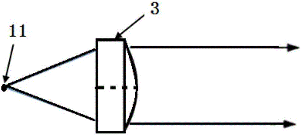
[0033] Embodiment 1, as Figure 4 , the multi-light-emitting point packaged semiconductor laser collimation device described in this example has a multi-light-point packaged diode 1 as an emission light source, and the multi-light-point packaged diode 1 has two light-emitting points; and is arranged on the multi-light-point packaged diode The collimating optical system on the beam exit path, the collimating optical system includes a microlens array composed of 2 microlenses 1 arranged in an array on the multi-spot package diode beam exit path and arranged on On the beam signal output path of each microlens I, there is a lens II capable of cooperating with the microlens I to collimate the emitted beam so as to output parallel light. Further, the center of any microlens I is located on the optical axis of the corresponding luminous point, and the distance between the microlens I and the luminous point is d=0.260mm, wherein the distance between the luminous point and the adjacent...

Embodiment 2

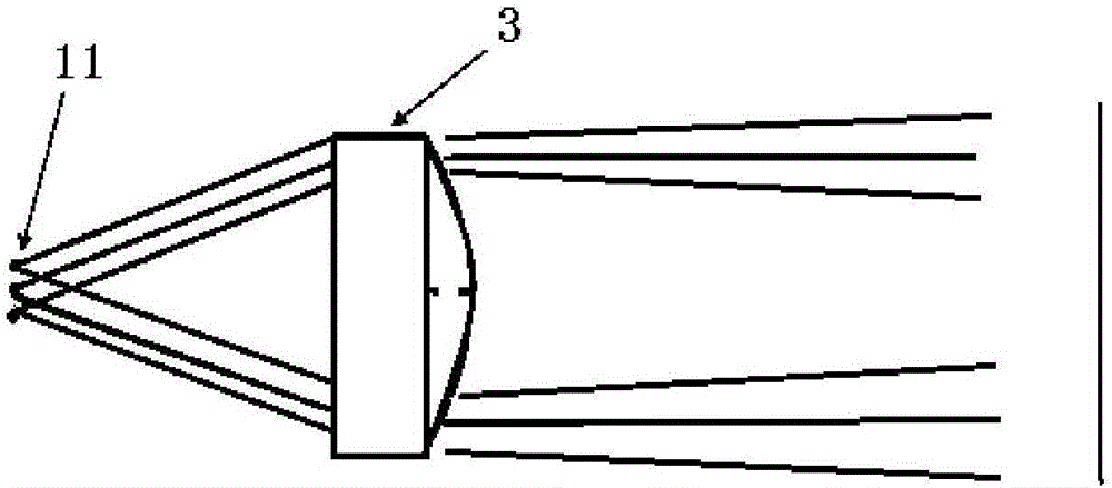
[0034] Embodiment 2, as Figure 5 , the multi-light-spot packaging semiconductor laser collimation device described in this example has a multi-light-spot package diode 1 as an emission light source, and the multi-light-spot package diode 1 has 4 light-emitting points; and is arranged on the multi-spot package diode The collimating optical system on the beam exit path, the collimating optical system includes a microlens array composed of 4 microlenses 1 arranged in an array on the multi-spot packaged diode beam exit path and arranged on On the light beam output path of each lens I, there is a lens II capable of collimating the emitted light beam with the micro lens I to output parallel light. Further, the center of any microlens I is located on the optical axis of the corresponding light-emitting point, and the distance between the lens I and the light-emitting point is d=0.179mm, wherein the distance a between the light-emitting point and the adjacent light-emitting point is...

Embodiment 3

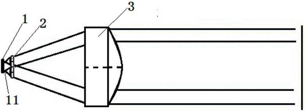
[0035] Embodiment 3, the laser projector described in this example, which is provided with the multi-light-emitting point packaging semiconductor laser collimation device in the optical structure, and the multi-light-emitting point packaging semiconductor laser collimation device includes a multi-light-emitting point package as the emission light source Diode 1, the multi-spot packaged diode 1 has 4 light-emitting points; The microlens array formed by the microlens I arranged in an array on the beam exit path of the point-package diode and the microlens array arranged on the beam exit path of each microlens I can cooperate with the lens I to collimate the emitted beam to output Lens II for Parallel Light. Further, the center of any one of the microlenses I is located on the optical axis of the corresponding luminous point, and the distance between the lens I and the luminous point is d=0.179mm, wherein the distance between the luminous point and the adjacent luminous point a ...


PUM


Abstract

The invention discloses a projection system with a multi-luminous-spot packaging semiconductor laser alignment structure. The projection system comprises a multi-luminous-spot packaging diode used as an emitting light source, and an alignment structure arranged on a light beam emission path of the multi-luminous-spot packaging diode, wherein the alignment structure comprises a micro lens array which consists of a plurality of micro lenses I that are in array configuration on the light beam emission path of the multi-luminous-spot packaging diode, and a lens group II which is arranged on the light beam emission path of each micro lens I and can perform alignment on the light beam emitted by the multi-luminous-spot packaging diode by matching with the micro lenses I; the number of the micro lenses I is determined according to the number of the luminous spots of the multi-luminous-spot packaging diode; and the sizes and the positions of the micro lenses are determined by the distances and the light beam angles of the luminous spots, namely each micro lens is only corresponding to one luminous spot light beam. According to the projection system, the alignment for the multi-luminous-spot packaging diode light beam is realized by adding the micro lens array before the existing alignment lens group, so that a relatively good alignment effect is realized without changing the existing alignment system condition.

Description

technical field [0001] The invention belongs to the technical field of laser collimation, and in particular relates to a projection system with a semiconductor laser collimation structure packaged with multiple light-emitting points. Background technique [0002] Semiconductor lasers are more and more used in the commercial field because of their small size, stability and ease of use. However, these characteristics also limit the power of semiconductor lasers. Generally speaking, the power of semiconductor lasers can only reach watts, such as 1- 2 watts, etc., in order to overcome this limitation and maximize the luminous power of semiconductor lasers, some semiconductor diode manufacturers now use a certain process technology to package the light-emitting points of two or more semiconductor diodes into one semiconductor diode. The distance between each light-emitting point is generally about several hundred microns. Although this method can improve the light-emitting power ...

Claims


Application Information

Patent Timeline
IPC IPC(8): G03B21/20G02B27/30
CPCG03B21/20G02B27/30
Inventor 孔维成付瑶孙阳杨思文杜健陈易廖明慧
Owner CHINA HUALU GRP
Why Eureka
Try Eureka