Semiconductor device

A semiconductor and program technology, used in computer security devices, instruments, computing, etc., to solve problems such as power supply noise and weak microcomputer resistance.

Active Publication Date: 2017-03-22
RENESAS ELECTRONICS CORP
View PDF7 Cites 2 Cited by
  • Summary
  • Abstract
  • Description
  • Claims
  • Application Information

AI Technical Summary

Problems solved by technology

But the problem that arises is that microcomputers are less resistant to such attacks, making repetitive power supply noise, etc.

Method used


Image

  • Semiconductor device
  • Semiconductor device
  • Semiconductor device

Examples


no. 1 example

[0047]

[0048] Although a plurality of embodiments will be described below, the semiconductor devices to be described in the respective embodiments are respectively sold according to new commercial sales models conceived by the present inventors. Here, a description will be made first about a semiconductor device business sales model conceived by the present inventors.

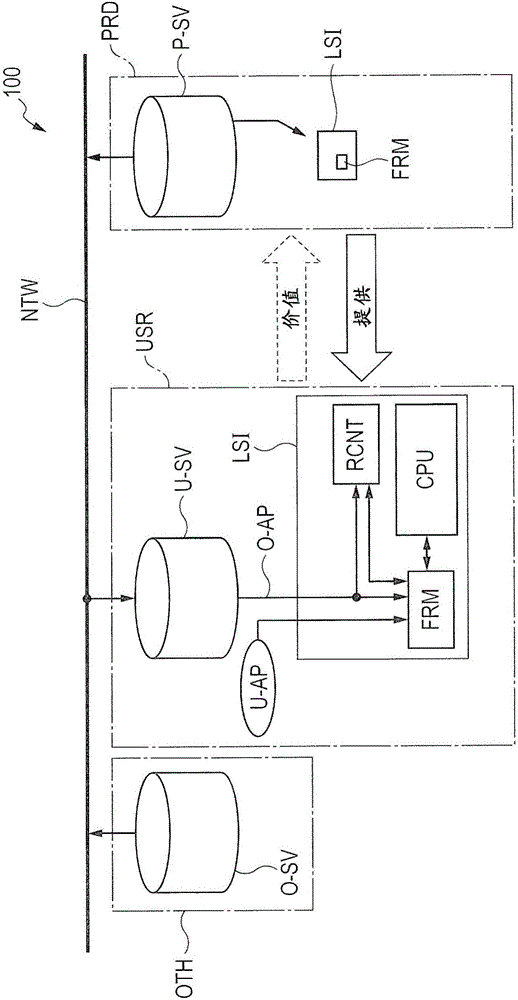
[0049] figure 1 is a system diagram showing the configuration of a semiconductor device commercial sales model according to the embodiment. In the same drawing, reference numeral 100 denotes a semiconductor device business sales model. Although not specifically shown, the semiconductor device business sales model 100 includes: a provider PRD, a user USR, and a third party OTH that provides programs.

[0050] The provider PRD sells the microcomputer LSI to the user USR. In a microcomputer LSI, a plurality of circuit blocks are formed in a single semiconductor chip by a known semiconductor manufacturing m...

no. 2 example

[0225] Figure 12 is a layout diagram showing the layout of data stored in the flash memory FRM according to the second embodiment.

[0226] The flash memory FRM according to the second embodiment is divided into a plurality of areas. In the area where the flash memory FRM is configured, Figure 12 The non-secure program area, secure program area, and protected information area are shown in . exist Figure 12 Among them, the non-secure program area is indicated by reference numeral 1200 , the secure program area is indicated by reference numeral 1201 , and the protected information area is indicated by reference numeral 1202 .

[0227] In the second embodiment, safety programs whose safety should be ensured are stored in the safety program area 1201 , and non-safety programs are stored in the non-safety program area 1200 . Information that protects the secure program area 1201 is stored in the protected information area 1202 .

[0228] In the new semiconductor business sa...

no. 3 example

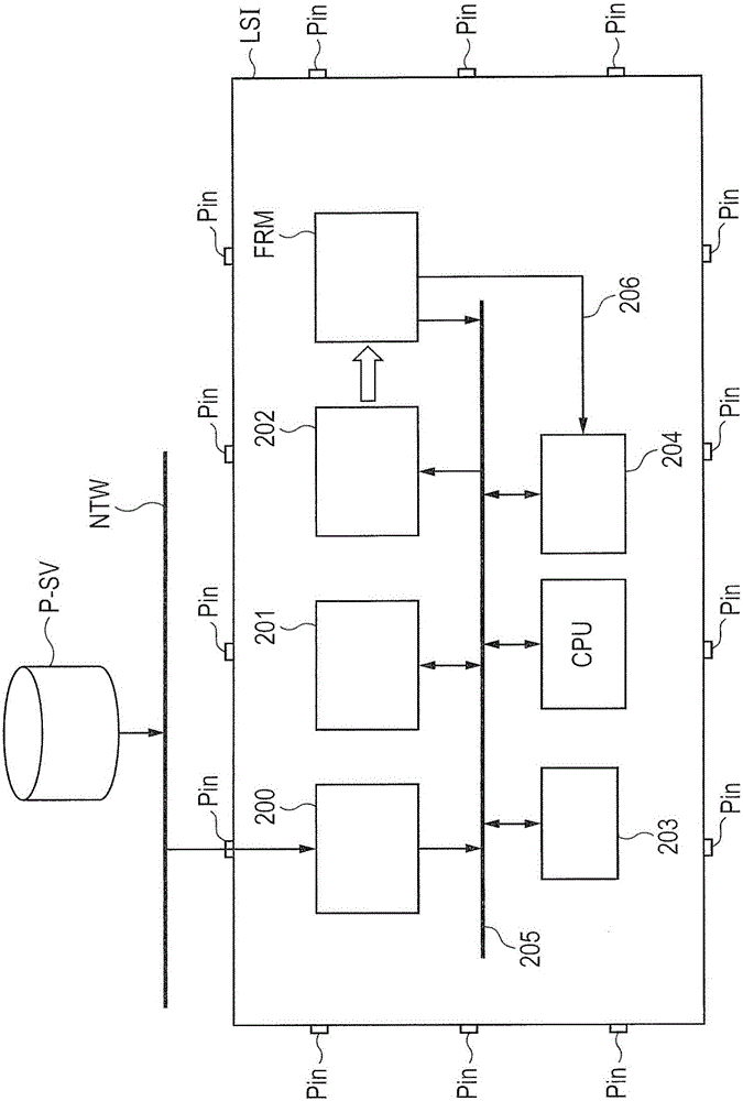
[0257] Figure 15 is a block diagram showing the configuration of a microcomputer according to the third embodiment. because Figure 15 The configuration of the microcomputer LSI shown is similar to figure 2 The microcomputers are shown, and the differences between them will be mainly described. In addition, in addition to microcomputer LSI, such as figure 2 as in Figure 15 Even server P-SV and network NTW are shown.

[0258] In the new semiconductor business sales model, such as figure 1 As shown, the provider PRD pre-writes a security program such as an RTOS into the flash memory FRM. A microcomputer LSI provided with a flash memory FRM in which an RTOS is written, a microprocessor CPU, and the like is sold from a provider PRD. The user USR writes the user program U-AP etc. generated by the user USR into the flash memory FRM in the purchased microcomputer LSI.

[0259] In this case, such as when the user USR performs version upgrade or corrects the inconvenience ...


PUM


Abstract

A semiconductor device capable of arbitrarily operating a microprocessor while protecting a secure program is provided. The semiconductor device includes a memory equipped with a first program area in which an arbitrary program is stored, and a second program area in which a secure program is stored, a microprocessor which outputs an address designating an instruction in a program, and a memory protection unit which controls access to the memory based on the address outputted from the microprocessor. When the address outputted from the microprocessor by executing the program in the first program area designates a branch allowable area in the second program area, the memory protection unit permits access to the memory. When the address designates a branch prohibition area, the memory protection unit inhibits access to the memory.

Description

[0001] Cross References to Related Applications [0002] The entire contents of Japanese Patent Application No. 2015-182140 filed on September 15, 2015, including specification, drawings and abstract, are incorporated herein by reference. technical field [0003] The present invention generally relates to a semiconductor device, and more particularly, to a semiconductor device having a microprocessor and an electrically rewritable nonvolatile memory each built into a single semiconductor chip. Background technique [0004] A semiconductor device including a microprocessor (hereinafter referred to as a central processing unit) and an electrically rewritable nonvolatile memory each built into a single semiconductor chip is known, for example, as a microprocessor. Such microprocessors are often used even in the field of products requiring safety. When a microcomputer is used in a product field requiring security, an attack against security is in principle performed from the o...

Claims


Application Information

Patent Timeline
Patent Type & Authority Applications(China)
IPC IPC(8): G06F21/57G06F21/74G06F21/78
CPCG06F21/577G06F21/74G06F21/78G06F2221/034G06F21/52G06F21/55G06F21/57G06F12/1408G06F12/1441G06F2212/1052G06F2212/402
Inventor 石原国泰植木浩
Owner RENESAS ELECTRONICS CORP
Why Eureka
Try Eureka